Memory chip, memory component and corresponding memory module and method

a memory chip and memory component technology, applied in the field of memory chips, a memory component and a corresponding memory module and method, to achieve the effect of simplifying storage and reading of specification information

Inactive Publication Date: 2005-09-20
POLARIS INNOVATIONS LTD
View PDF8 Cites 11 Cited by
  • Summary
  • Abstract
  • Description
  • Claims
  • Application Information

AI Technical Summary

Benefits of technology

[0010]It is the object of the present invention to create a memory chip, a memory component and a corresponding memory module and method, in which the storage and reading of the specification information are simplified.
[0014]The object according to the invention brings with it a simplified and lower-cost design of the memory module, since the EPROM memory previously required becomes superfluous. This results in higher reliability and a lower risk of producing faulty modules caused by poor solder joints.

Problems solved by technology

Furthermore, it is generally known to replace faulty storage capacitors in such memory chips SB with redundant storage capacitors using fuses or anti-fuses, as they are known.

Method used


Image

  • Memory chip, memory component and corresponding memory module and method
  • Memory chip, memory component and corresponding memory module and method
  • Memory chip, memory component and corresponding memory module and method

Examples


first embodiment

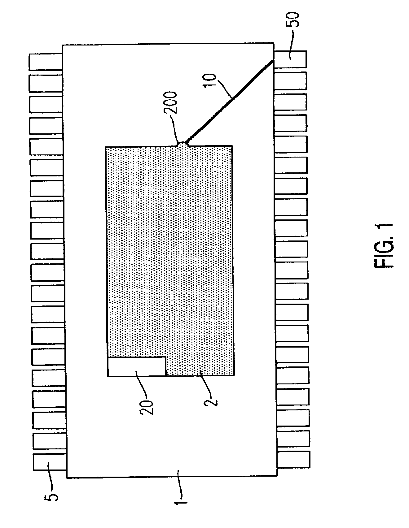
[0025]FIG. 1 shows a schematic representation of a memory component in silicon technology as first embodiment of the present invention.

[0026]In FIG. 1, reference 1 refers to a memory component having a TSOP package, which component contains a memory chip 2 that is connected to connections 5 of the memory component 1 via circuitry that is not shown, e.g. via a leadframe. The memory chip 2 contains a multiplicity of memory cells, for example SDRAM memory cells, plus an area or an array 20 having a multiplicity of fuses, which can be written to and read individually in order to store specification information.

[0027]In particular, the memory chip 2 has a connection 200 for serial reading of the array 20, from which a data line 10 is taken to a connection pin 50. This data line is a serial, internal data line, via which, in a specific test mode, the specification information stored in the fuse array 20 can be read or written via the connection pin 50.

[0028]In the first embodiment, the da...

second embodiment

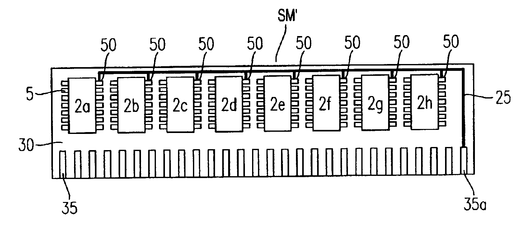
[0029]FIG. 2 shows a schematic representation of a memory module having a multiplicity of memory components as second embodiment of the present invention.

[0030]In FIG. 2, reference SM′ refers to a memory module having a multiplicity of memory components 2a to 2h, which are mounted on a printed circuit board 30 having circuitry that is not shown. The printed circuit board 30 has contacts 35, which are connected to the connection pins 5 of the memory components via the circuitry that is not shown. A specially reserved contact 35A is connected to the connection pin 50 of the memory chips 2a to 2h via a data bus 25, so that the specification information from all the memory components 2a to 2h can be taken to the contact 35A via the data bus, and thus can be read externally by a computer in which the memory module is installed.

third embodiment

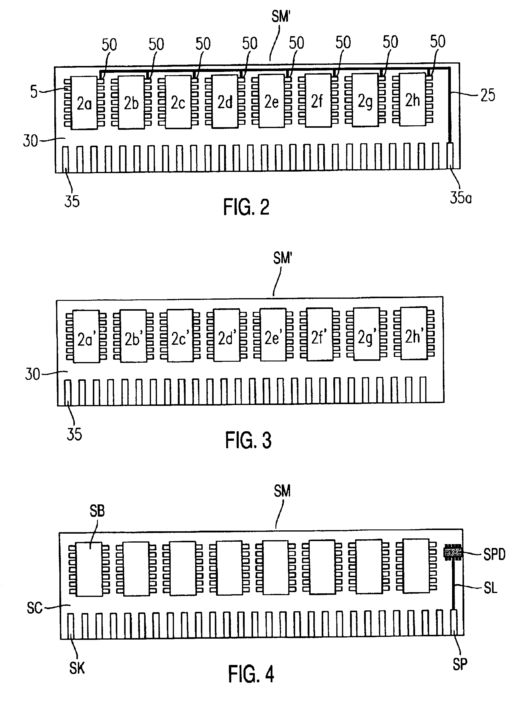
[0031]FIG. 3 shows a schematic representation of a memory module having a multiplicity of memory components as third embodiment of the present invention.

[0032]In the memory module SM′ shown in FIG. 3, no connection pin 50 is provided on the memory components 2a′ to 2h′, and thus the additional contact 35A on the printed circuit board 30 is also omitted. In this second embodiment, the specification information from the fuse array 20 can be read or programmed via appropriate addressing of the normal address lines of the memory cells in a given special test mode. This reduces the number of contacts on the printed circuit board.

[0033]Hence in the second embodiment, after starting up the memory module, the reading process can be initiated by a special test mode, or the writing process can be initiated by another special test mode, whereupon the specification information is output via the normal connection pin 5 for data. This has the advantage that then extra pins are no longer needed fo...


PUM


Abstract

The present invention creates a memory chip, a memory component and a corresponding memory module. The memory chip is equipped with a multiplicity of memory cells and has an an [sic] array (20) of fuses and anti-fuses respectively, which can be written to and read individually in order to store specification information.

Description

TECHNICAL FIELD[0001]The present invention relates to a memory chip, a memory component and a corresponding memory module and method.BACKGROUND ART[0002]Here, memory component is intended to mean one or more memory chips packaged in a single package (e.g. TSOP package), and a memory module is intended to mean one or more memory components mounted on a printed circuit board.[0003]Although applicable to any integrated circuits in principle, the present invention and the problems on which it is based are explained with reference to integrated memory chips in silicon technology.[0004]FIG. 4 shows a schematic representation of a known memory module having a multiplicity of memory components, each containing a memory chip in silicon technology.[0005]In FIG. 4, SC refers to a circuit board, on which, in order to form a memory module SM, a multiplicity of packaged memory chips, or rather memory components SB, are mounted and wired up to contacts SK to form a memory module SM.[0006]According...

Claims


Application Information

Patent Timeline
Patent Type & Authority Patents(United States)
IPC IPC(8): G11C17/14G11C17/16
CPCG11C17/16
Inventor SCHNELL, MARTIN
Owner POLARIS INNOVATIONS LTD
Why Eureka
Try Eureka