Storage of an image in an integrated circuit

an integrated circuit and image technology, applied in the field of integrated circuits, can solve the problems of inability to read, incompatible with the manufacturing of integrated circuits at an industrial scale, and inability to store images, and achieve the effect of reducing costs on an industrial scal

Active Publication Date: 2013-01-01
STMICROELECTRONICS (ROUSSET) SAS
View PDF4 Cites 4 Cited by
  • Summary
  • Abstract
  • Description
  • Claims
  • Application Information

AI Technical Summary

Benefits of technology

[0010]A method for permanently storing an image at the level of an integrated circuit is disclosed, the image remaining accessible when the integrated circuit is disabled, where the image storage can be performed simply and at a decreased cost an industrial scale.
[0012]Another object of an embodiment of the invention is to make the reading of the image stored at the level of the integrated circuit particularly simple.
[0013]Embodiments of present invention also aim at an integrated circuit at the level of which an image is permanently stored, the image remaining accessible when the integrated circuit is disabled, where the image can be read in a simple way.

Problems solved by technology

A disadvantage is that the image to be stored may be unavailable at the time when the etch masks used during the integrated circuit manufacturing are defined.
Since the storage of data in a ROM generally requires the use of at least one specific mask for the forming of the memory cell connections, it is not compatible, for a manufacturing of circuits at an industrial scale, to have to multiply the number of masks to be used.
When the image is stored in a ROM, an EEPROM, etc., it is no longer possible to read it when the circuit is no longer functional.
However, such a method needs to be implemented separately on each integrated circuit and is thus not compatible with the manufacturing of integrated circuits at an industrial scale.
Further, the images to be stored may be unavailable at the time when the laser etch method is to be implemented.

Method used


Image

  • Storage of an image in an integrated circuit
  • Storage of an image in an integrated circuit
  • Storage of an image in an integrated circuit

Examples


Embodiment Construction

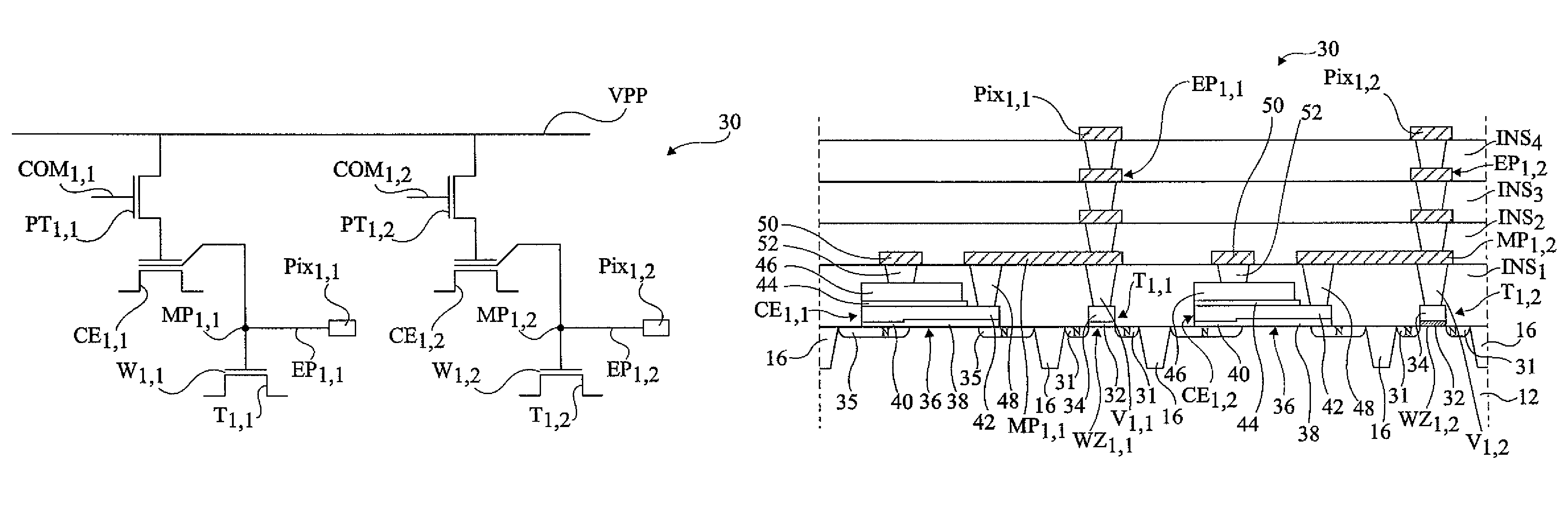
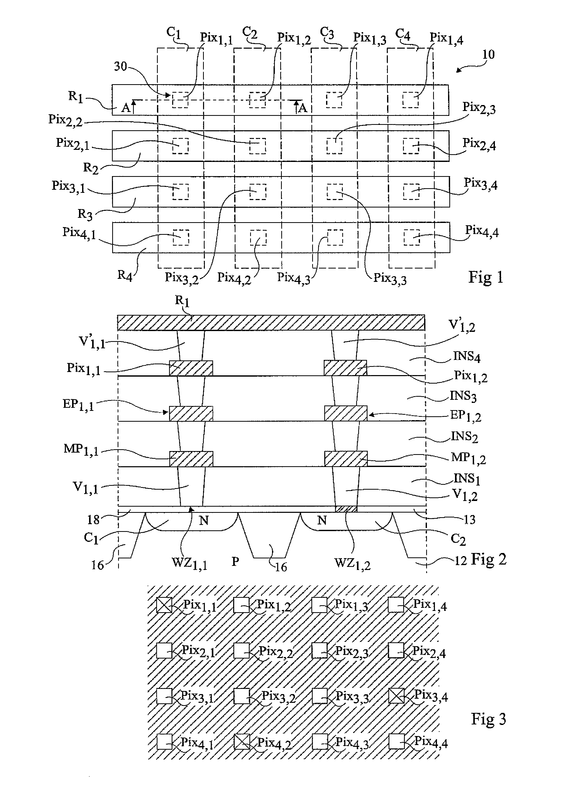
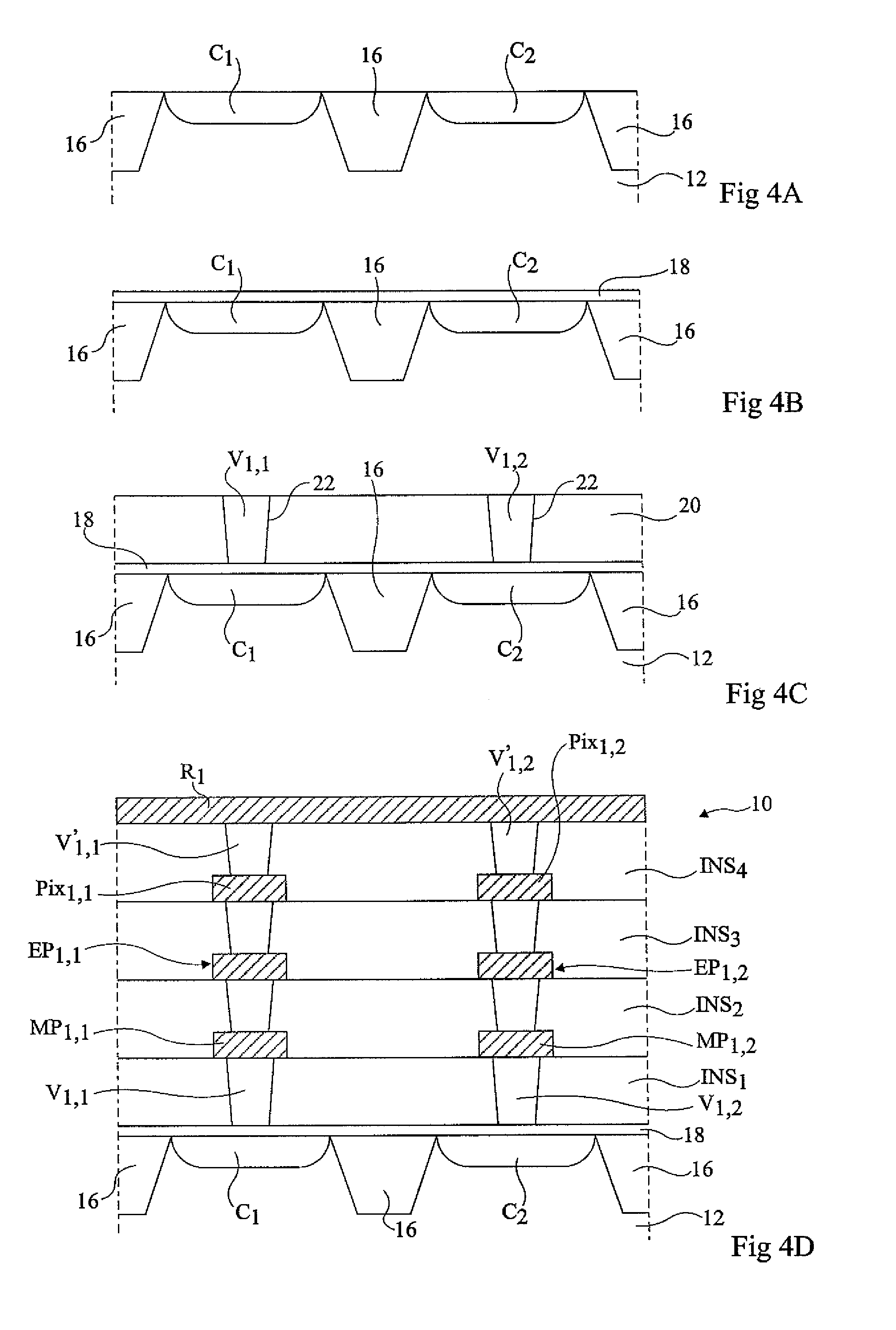
[0036]For clarity, only those steps and elements which are useful to the understanding of the present invention have been shown and will be described. Further, the same elements have been designated with the same reference numerals in the different drawings and, moreover, as usual in the representation of integrated circuits, the various drawings are not to scale.

[0037]In the following description, the assembly of metal tracks simultaneously formed during the integrated circuit manufacturing process is called a metallization level. These may be metal tracks lying at the surface of an insulating layer or leveling the surface of an insulating layer. A conductive portion crossing an insulating layer and connecting a metal track of a given metallization level to a metal track of an adjacent metallization level is called a via. The assembly of vias simultaneously formed during the integrated circuit manufacturing process is called a via level. Vias may be formed simultaneously to the met...


PUM


Abstract

An integrated circuit including a substrate of a semiconductor material and first metal portions of a first metallization level or of a first via level defining pixels of an image. The pixels are distributed in first pixels, for each of which the first metal portion is connected to the substrate, and in second pixels, for each of which the first metal portion is separated from the substrate by at least one insulating portion.

Description

CROSS REFERENCE TO RELATED APPLICATIONS[0001]This application claims the priority benefit of French patent application Ser. No. 08 / 55628, filed on Aug. 19, 2008, entitled “STORAGE OF AN IMAGE IN AN INTEGRATED CIRCUIT,” which is hereby incorporated by reference to the maximum extent allowable by law.BACKGROUND OF THE INVENTION[0002]1. Field of the Invention[0003]The present disclosure generally relates to integrated circuits and, more specifically, to the non-volatile storage of an image in an integrated circuit during the circuit manufacturing.[0004]2. Discussion of the Related Art[0005]In many cases, it is needed to permanently store an image in an integrated circuit on manufacturing of the integrated circuit. The image for example shows an identifier of the wafer on which the integrated circuit is manufactured, the position of the integrated circuit on the wafer, an identifier of the wafer batch to which the wafer of the integrated circuit belongs, etc.[0006]Generally, to permanen...

Claims


Application Information

Patent Timeline
Patent Type & Authority Patents(United States)
IPC IPC(8): H01L27/15H01L31/12H01L29/26H01L33/00
CPCG11C17/16H01L27/101H01L27/105H01L27/115H01L27/11521H10B69/00H10B41/30
Inventor FORNARA, PASCALMARINET, FABRICE
Owner STMICROELECTRONICS (ROUSSET) SAS
Why Eureka
Try Eureka