
Method for mass production of a plurality of magnetic sensors

a technology of magnetic sensors and mass production, applied in the field of methods, can solve the problems of not being able to produce components with an amorphous structure, the detection and measurement of magnetic fields of devices, and the day has been resolved in a satisfactory fashion, and achieves the effects of facilitating the adhesion of the film, reducing the cost price, and great uniformity

Inactive Publication Date: 2005-09-27
ASULAB SA
View PDF10 Cites 18 Cited by
  • Summary
  • Abstract
  • Description
  • Claims
  • Application Information

AI Technical Summary

Benefits of technology

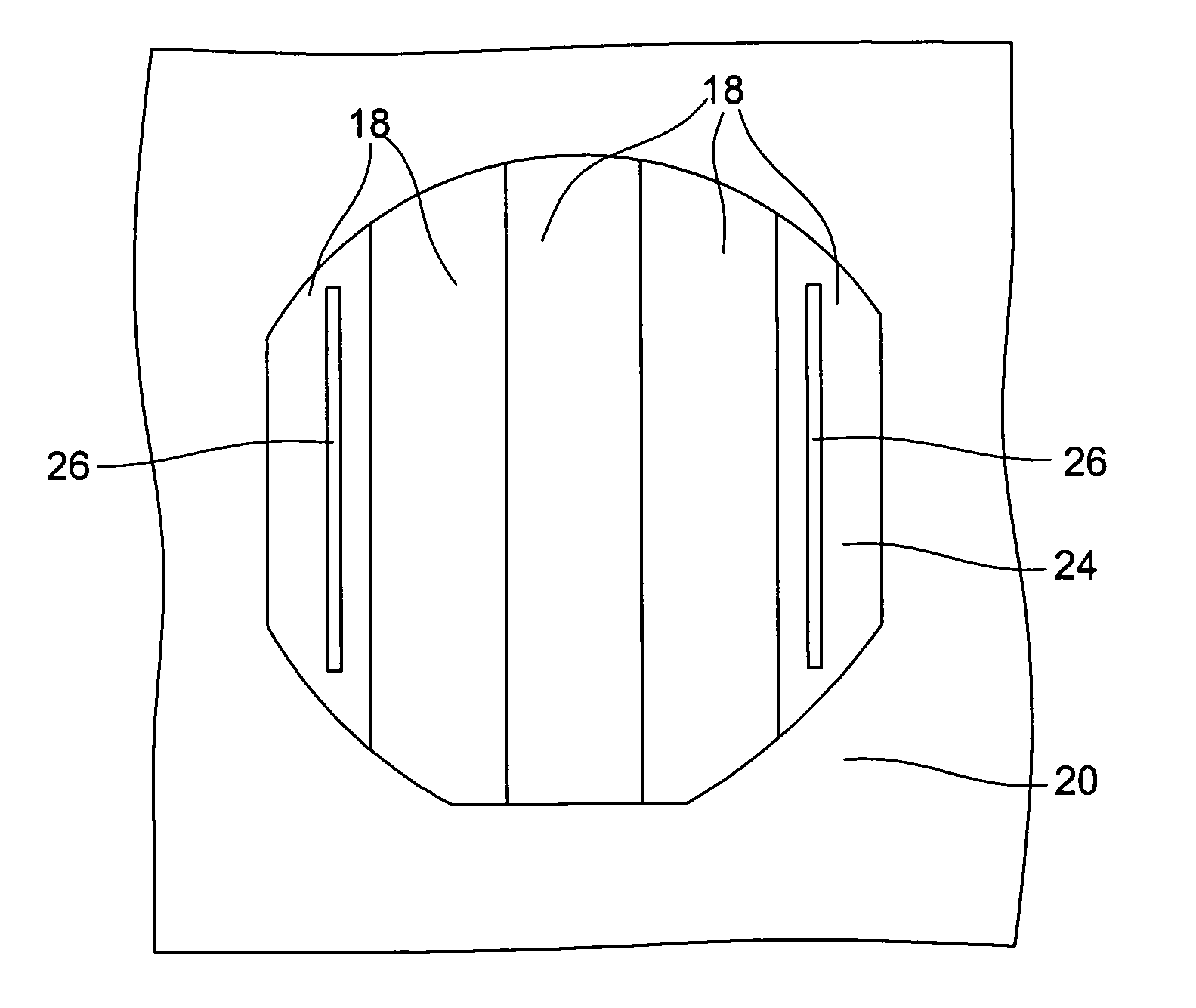
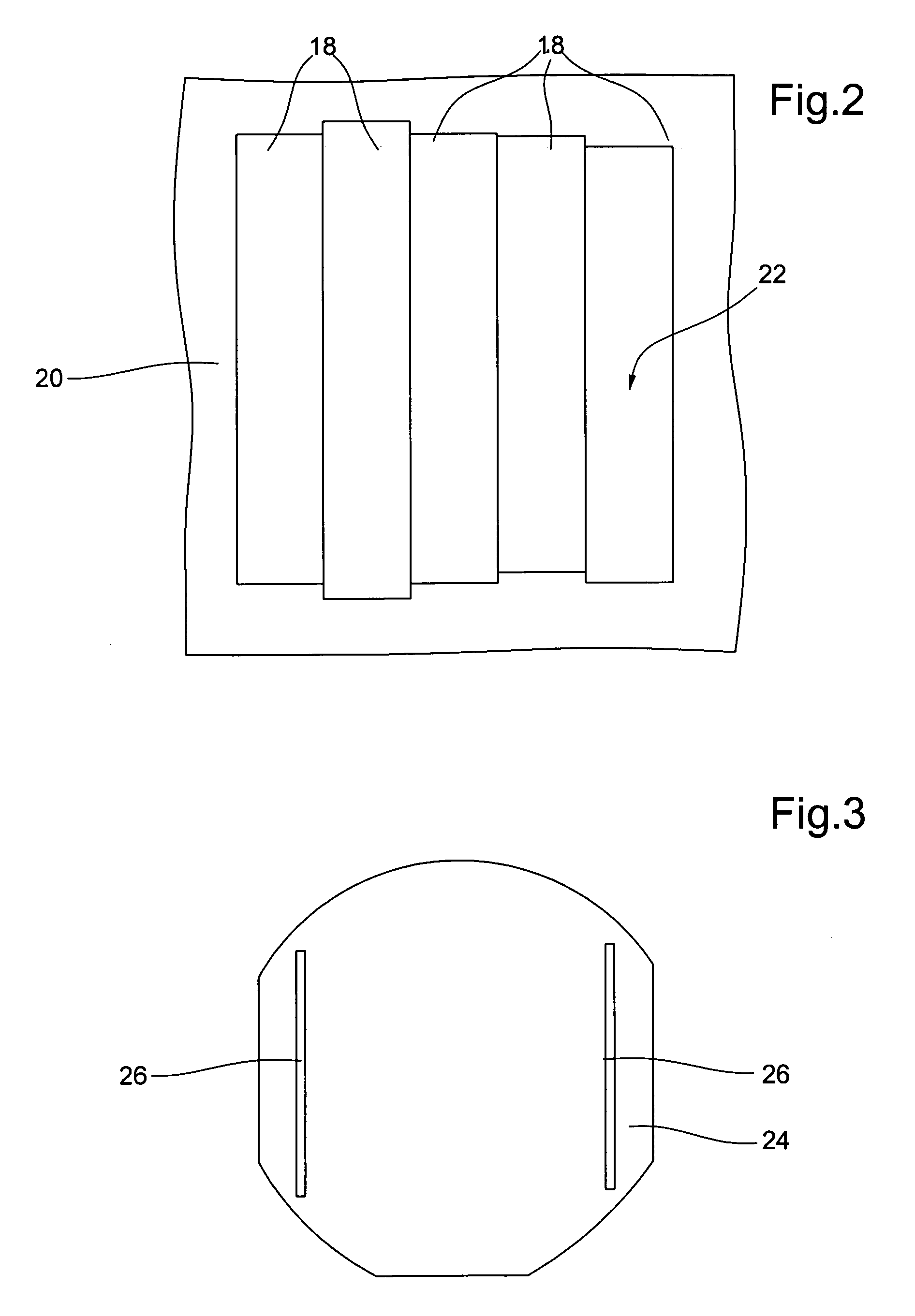
[0017]Thanks to these features, the present invention provides a method which allows production of all the operations for producing magnetic sensors with amorphous magnetic cores on the board made of semiconductor material, in which the electronic circuits which are intended to be associated with said magnetic sensors are integrated. It is possible in particular, thanks to the present invention, to produce in series the magnetic cores produced in an amorphous magnetic material and to saw the board of semiconductor material only once the magnetic sensors have been entirely completed. Such a method therefore allows simultaneous production of large quantities of magnetic sensors, typically of the order of 3000 sensors or more per semiconductor board of 6 inches, in an extremely reliable manner and at a low cost price. It was realised in particular that the possible misalignment between cores and coils did not exceed a few microns, and that the characteristics of the magnetic sensors showed great uniformity over the same board, and even over a series of boards. These particularly advantageous results are achieved thanks to the fact that, according to the present invention, a film is formed by means of a plurality of bands of an amorphous magnetic material, such as is commercially available, disposed one beside the other on a support, this film then being glued onto the board of semiconductor material then structured in order to form the magnetic cores before the board is finally sawn in order to provide a plurality of individual sensors which are ready for use. Such a technique is of course much more advantageous than the techniques of prior art which comprised, after having integrated the electronic circuits, cutting up the board of semiconductor material then structuring one by one the magnetic cores on the individual circuits.
[0018]According to another feature of the invention, the film of amorphous magnetic material is glued in a vacuum on the semiconductor substrate. It is thus ensured that the film will be applied on the semiconductor substrate with a considerable force, which assists adhesion of the film on the substrate and allows the avoidance of air bubbles being trapped under the metallic layer.
[0019]According to yet another feature of the invention, the film of amorphous magnetic material is structured by means of engraving techniques which are currently employed in the field of semiconductor component production. Reliable techniques are therefore implemented which allow production of magnetic cores at a low cost price and ensure excellent reproducibility of the features of these cores.

Problems solved by technology

The production of such devices for detection and measurement of magnetic fields poses a great problem which, as far as the applicant knows, has not to this day been resolved in a satisfactory fashion.
Now, none of the currently available techniques for producing semiconductor devices allows components with an amorphous structure to be produced.
Hence, the techniques for producing CMOS integrated circuits only allow production of components with an ordered crystalline structure, and they are unable to propose replacement solutions for developing bodies with an amorphous structure, i.e. not having a crystal lattice.
These techniques only permit however deposition of materials which have a simple chemical composition formed by a single component.
It will be readily understood that such a technique, if it can be used at the experimental stage, is in no way applicable on an industrial scale where very large quantities of components must be able to be produced rapidly and at low cost.

Method used


Image

  • Method for mass production of a plurality of magnetic sensors
  • Method for mass production of a plurality of magnetic sensors
  • Method for mass production of a plurality of magnetic sensors

Examples


Embodiment Construction

[0028]The present invention starts with the general inventive concept which comprises forming a film of amorphous magnetic material by means of a plurality of bands of amorphous magnetic material which are disposed one beside the other on a support and gluing the thus obtained film on a semiconductor board, in which the electronic circuits associated with the magnetic sensors which are intended to be produced have been previously integrated. After this gluing step, the film of amorphous magnetic material is structured by etching in order to form the magnetic cores which form the part of the magnetic sensors sensitive to the exterior magnetic field. Thanks to these features, the problem posed by the techniques currently available for production of semiconductor devices which do not allow production of amorphous layers is resolved, and the production in series of magnetic sensors with amorphous magnetic cores is made possible.

[0029]The present invention will be described in conjunctio...


PUM


Abstract

The present invention relates to a method for producing in large numbers a multiplicity of magnetic sensors produced on a semiconductor substrate, these sensors comprising at least one magnetic core produced in an amorphous magnetic material, characterised in that, after integration of the electronic circuits associated with the magnetic sensors, a film of amorphous magnetic material is glued onto the semiconductor substrate, this film being obtained from a band of amorphous magnetic material cut into a plurality of sections which are disposed one beside the other on a support, said film being then structured in order to form the magnetic cores of said magnetic sensors, the semiconductor substrate being finally cut up in order to provide a plurality of individual magnetic sensors.

Description

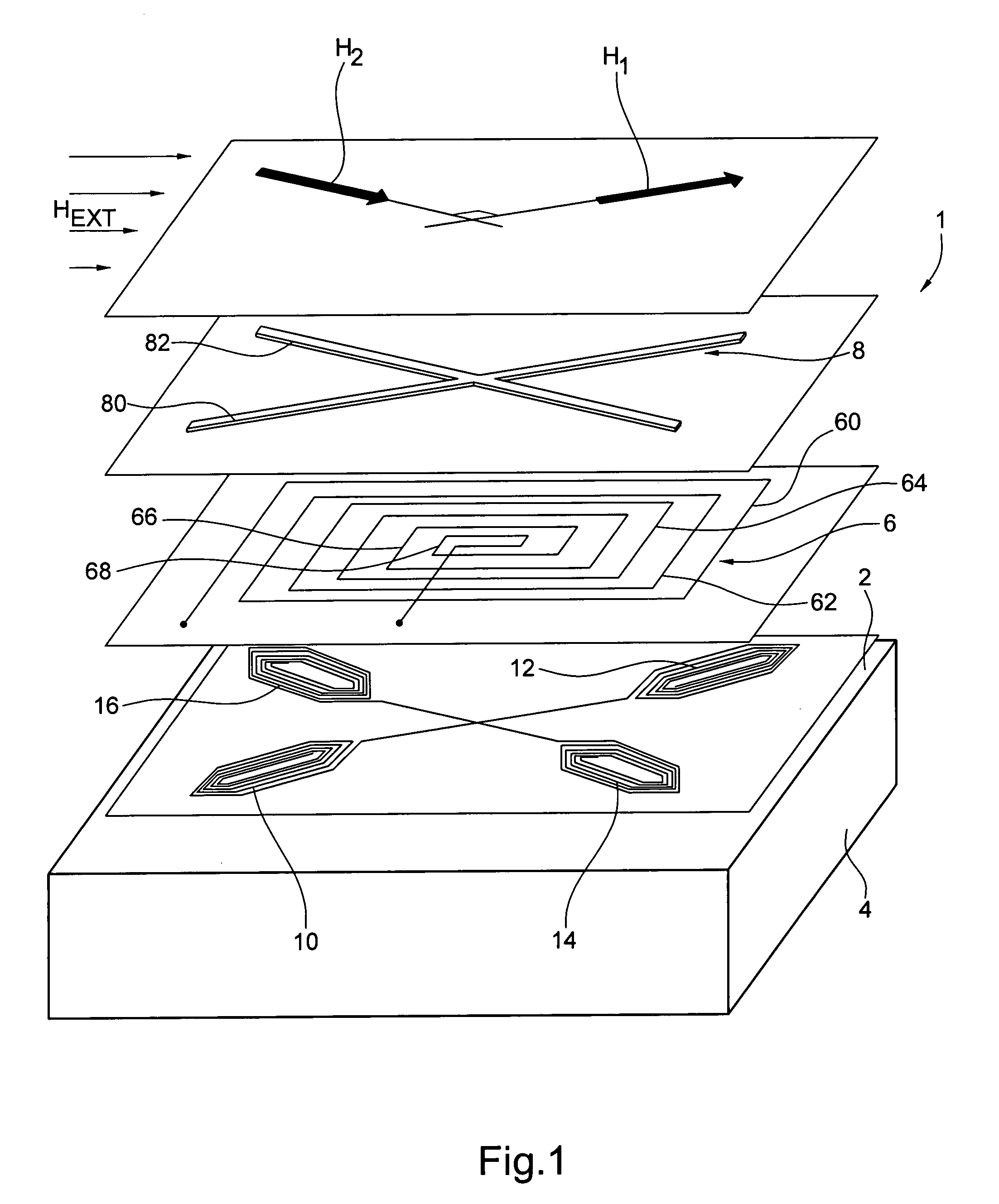
[0001]This is a National Phase Application in the United States of International Patent Application No. PCT / EP02 / 05753 filed May 22, 2002, which claims priority on European Patent Application No. 01202262.0, filed Jun. 12, 2001. The entire disclosures of the above patent applications are hereby incorporated by reference.FIELD OF THE INVENTION[0002]The present invention relates to a method of producing in large numbers a multiplicity of magnetic sensors. It relates in particular, but not exclusively, to magnetic sensors of the type described in the patent application EP 1 052 519 in the name of the applicant.BACKGROUND OF THE INVENTION[0003]A magnetic sensor of the above-mentioned type is represented in perspective and exploded in FIG. 1 which is appended to the present patent application. Designated overall by the general numerical reference 1, this magnetic sensor is mounted on the surface 2 of a semiconductor substrate 4 of a substantially parallelepiped shape. An electronic circu...

Claims


Application Information

Patent Timeline
Patent Type & Authority Patents(United States)
IPC IPC(8): H01L43/00H01L43/12H10N50/01H10N50/10
CPCH01L43/12H10N50/01
Inventor PIGUET, DOMINIQUEVINCENT, FRANCK
Owner ASULAB SA
Learn More