Semiconductor memory device and electronic apparatus mounting the same

a memory device and semiconductor technology, applied in the direction of information storage, static storage, digital storage, etc., can solve the problems of limited operating lifetime of ferroelectric memory devices, difficult to increase the rewritable number of times of ferroelectric capacitors, and degraded ferroelectric films in the ability to exhibit distinct polarization, etc., to achieve long data retention lifetime and increase the rewritable number of times

Inactive Publication Date: 2005-09-27
PANASONIC CORP
View PDF7 Cites 2 Cited by
  • Summary
  • Abstract
  • Description
  • Claims
  • Application Information

AI Technical Summary

Benefits of technology

[0031]In view of the foregoing, it is therefore an object of the present invention to increase the rewritable number of times of

Problems solved by technology

However, since the phenomenon of polarization fatigue is observed in a ferroelectric film, the ferromagnetic film is degraded in the ability to exhibit distinct polarization if the operation of inverting the polarization is repeated.
If the writing or reading of data is repeatedly performed in the conventional ferroelectric memory device, the problem is encountered that the

Method used


Image

  • Semiconductor memory device and electronic apparatus mounting the same
  • Semiconductor memory device and electronic apparatus mounting the same
  • Semiconductor memory device and electronic apparatus mounting the same

Examples


embodiment 1

[0072]A semiconductor memory device according to a first embodiment of the present invention will be described herein below.

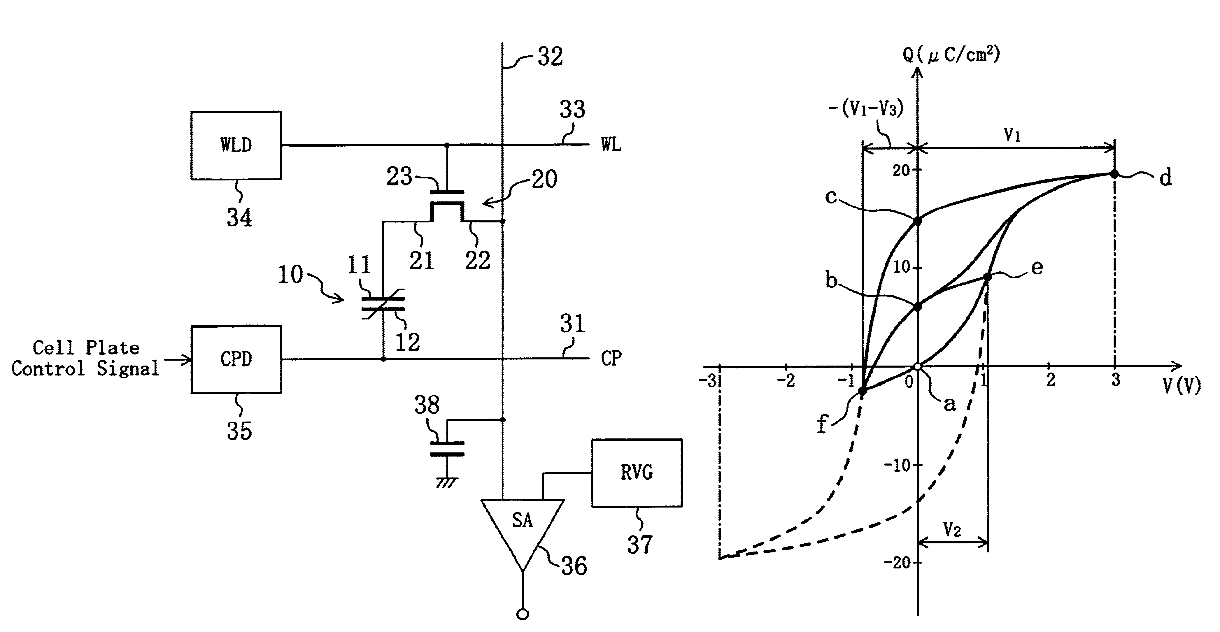
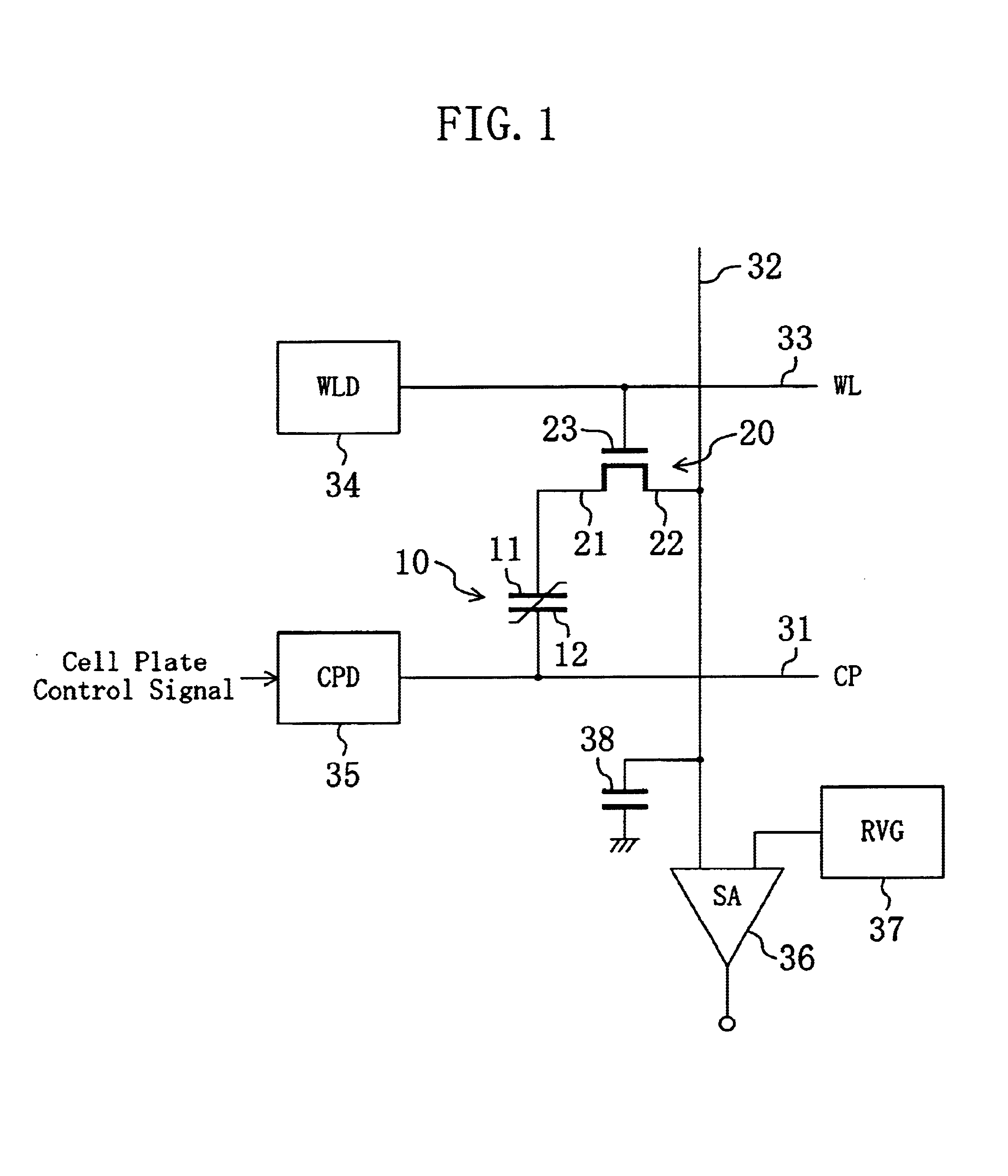
[0073]FIG. 1 shows a memory cell composing the semiconductor device according to the first embodiment. As shown in FIG. 1, the memory cell has a ferroelectric capacitor 10 and a transistor 20. The ferroelectric capacitor 10 has a ferroelectric film composed of SrBi2Ta2O9 with a thickness of 200 nm. The ferroelectric capacitor 10 has a first electrode 11 connected to the source 21 of the transistor 20 and a second electrode 12 connected to a cell plate line 31. The transistor 20 has a drain 22 connected to a bit line 32 and a gate electrode 23 connected to a word line 33.

[0074]In FIG. 1, 34 denotes a word line driver (WLD) for selecting the word line 33, 35 denotes a cell plate driver (CPD) for driving a cell plate line 31, and 36 denotes a sense amplifier (SA) for differentially amplifying a voltage on a bit line 32, 37 denotes a reference voltage generating ci...

embodiment 2

[0096]An electronic apparatus according to a second embodiment of the present invention will be described herein below.

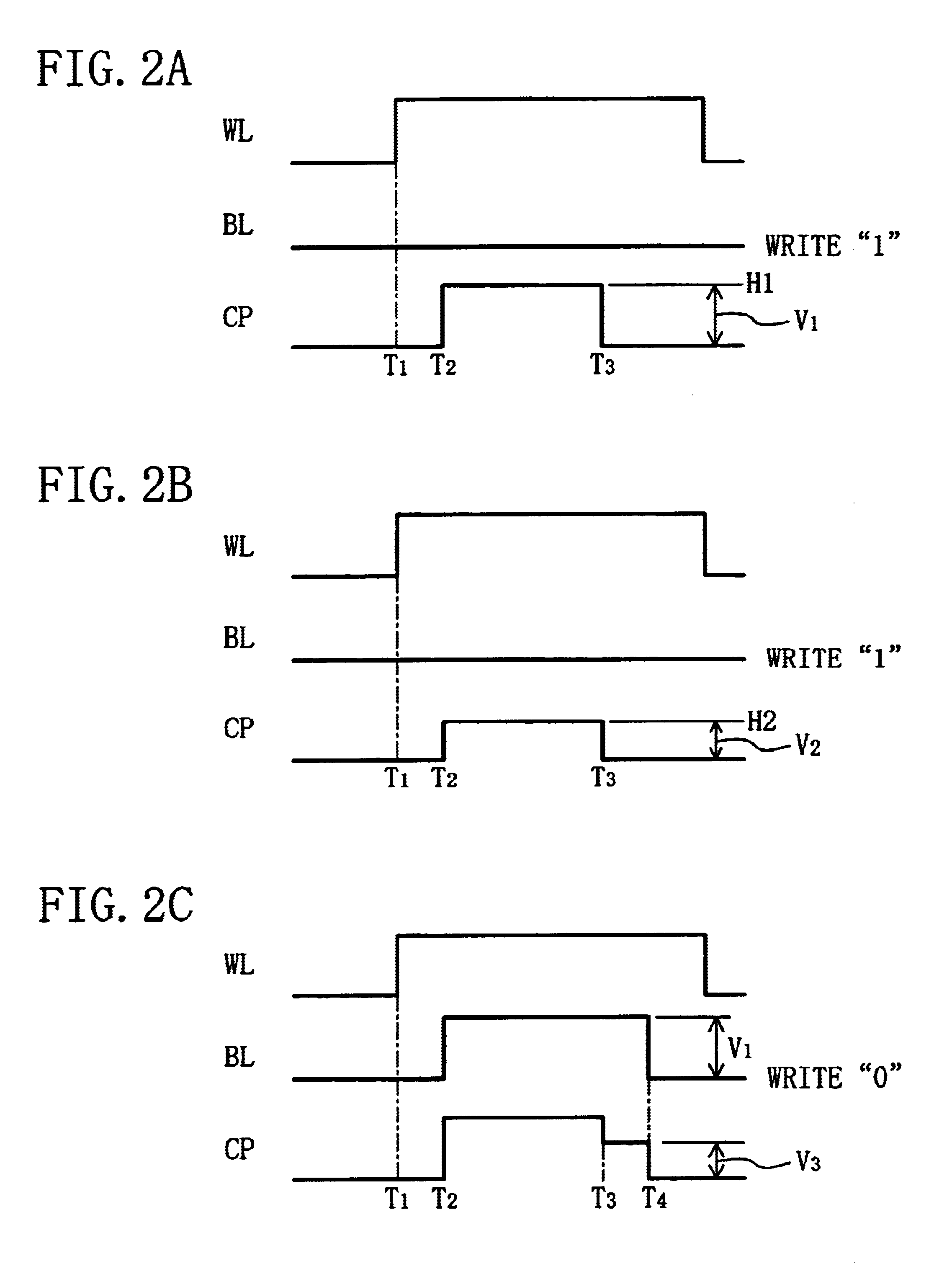
[0097]If the semiconductor memory device according to the first embodiment is mounted on a mobile electronic apparatus which operates with a rechargeable secondary battery, data once written should be retained over a long period of time when the power source of the mobile electronic apparatus is brought into a halted state or during the period during which the power source is disconnected from the electronic apparatus.

[0098]Accordingly, if a write operation is performed with a voltage which sufficiently elongates the retention period of a part or whole of written data immediately before the power source of the mobile electronic apparatus is halted or disconnected, a write voltage which allows the storage of data only during the period from the time the operation is initiated by turning on the power source till the power source is turned off is sufficient as the writ...


PUM


Abstract

In a ferroelectric capacitor, two displacements (points b and c) of a remanent polarization correspond to data “1” and one displacement (point a) of the remanent polarization corresponds to data “0”. When the data “1” is written, either of two electric voltage pulses different in potential or in pulse width is applied to the ferroelectric capacitor to position the displacement of the remanent polarization in the ferroelectric capacitor at the point b or at the point c. When the data “0” is written, on the other hand, the displacement of the remanent polarization in the ferroelectric capacitor is positioned at the point a.

Description

BACKGROUND OF THE INVENTION[0001]The present invention relates to a semiconductor memory device for storing data by using a ferroelectric capacitor in a part of a memory cell and to an electronic apparatus mounting the semiconductor memory device.[0002]As an example of a conventional semiconductor memory device having a memory cell composed of a ferroelectric capacitor and a transistor, there has been known one having a structure as shown in FIG. 10. As shown in FIG. 10, the memory cell of the semiconductor memory device has a ferroelectric capacitor 10 and a transistor 20. The ferroelectric capacitor 10 has a ferroelectric film composed of SrBi2Ta2O9 with a thickness of 200 nm. The ferroelectric capacitor 10 has a first electrode 11 connected to the source 21 of the transistor 20 and a second electrode 12 connected to a cell plate line 31. The transistor 20 has a drain 22 connected to a bit line 32 and a gate electrode 23 connected to a word line 33.[0003]In FIG. 10, 34 denotes a w...

Claims


Application Information

Patent Timeline
IPC IPC(8): G11C11/22
CPCG11C11/22
Inventor SHIMADA, YASUHIROKATO, YOSHIHISAYAMADA, TAKAYOSHI
Owner PANASONIC CORP
Why Eureka
Try Eureka