Apparatus for thermal compensation of an arrayed waveguide grating

an arrayed waveguide and thermal compensation technology, applied in the field of arrayed waveguide gratings, can solve the problems of affecting the performance of many devices, introducing substantial loss into the network, and malfunctioning the entire network,

Inactive Publication Date: 2005-10-11
INTEL CORP
View PDF14 Cites 23 Cited by
  • Summary
  • Abstract
  • Description
  • Claims
  • Application Information

AI Technical Summary

Problems solved by technology

Though designs vary depending on size, complexity and other factors, these networks are generally a complex system of interconnected optical components that perform signal input / output, switching, data processing, data analysis, and other functions.
Unfortunately, temperature variations affect the performance of many devices.
Affected devices may introduce substantial loss into a network due to signal degradation and, in a worst-case scenario, may result in malfunction of the entire network.
Many devices, such as arrayed waveguide gratings (AWGs), are susceptible to this detrimental temperature dependence.
This channel separation depends upon the phase differences in the waveguide array, which makes AWGs very sensitive to environmental effects.
Undesirably large amounts of power are required to run these devices, however.
Yet, these are expensive to fabricate and have inherent losses (both polarization independent and dependent loss).
Also, their operative temperature ranges are limited due to linearity and temperature dependent losses.
Reflection losses also limit device performance.
These approaches, however, have numerous problems.
Accurately mounting and positioning the fiber support arm to the fiber is difficult.
Further, fine-tuning support arm movement often requires complex structures, and, even with these, the fine-movement required is still not readily achievable.
Also, there is nothing to prevent the support arm from moving vertically out of the plane of the AWG.
Additionally, fabrication costs are high and stiction is a problem.
Device scalability is also limited.
And, for these designs and all of the above-described designs, the inherent losses are so great that larger-scale AWGs are not feasible.

Method used


Image

  • Apparatus for thermal compensation of an arrayed waveguide grating
  • Apparatus for thermal compensation of an arrayed waveguide grating
  • Apparatus for thermal compensation of an arrayed waveguide grating

Examples


Embodiment Construction

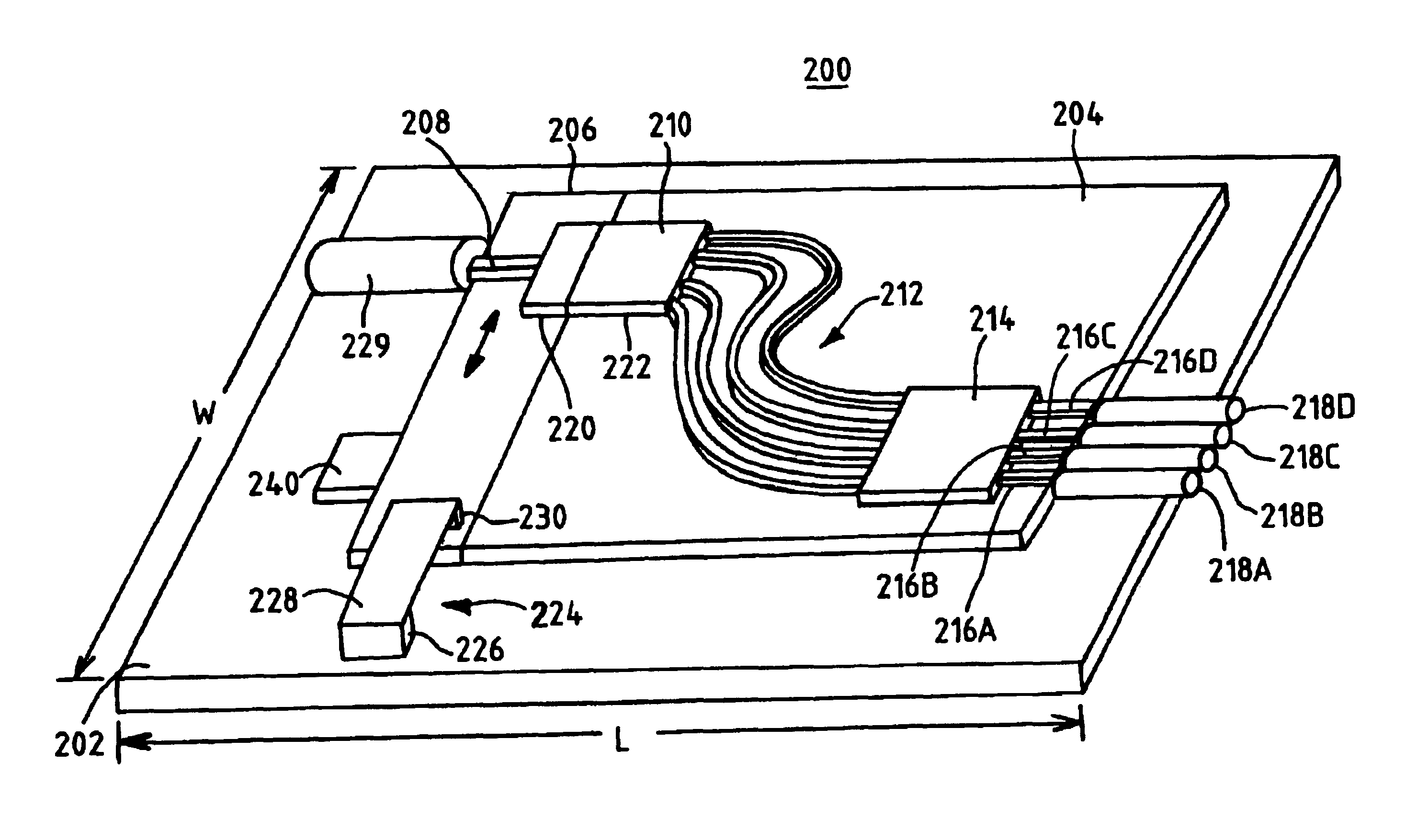
[0021]While preferred examples and numerous alternatives thereto are provided below, it will be appreciated by persons of ordinary skill in the art that these are merely examples and not intended to be exhaustive. On the contrary, the teachings herein may be used to form a great many arrayed waveguide gratings (AWGs) and other optical structures employing AWGs. Further, while the descriptions provided below are generally in the context of demultiplexer operation, the devices herein are reciprocal structures that may function as multiplexers, as well. Further still, while the approaches are described in the context of forming 1×N and N×N devices, with N equal to 4 in the depicted examples, the teachings herein may be used to form structures with N greater than 4, including structures with N much greater than 4. In fact, one of the advantages to the disclosed examples is that simple-to-fabricate-and-operate AWGs may now be formed with higher N-values.

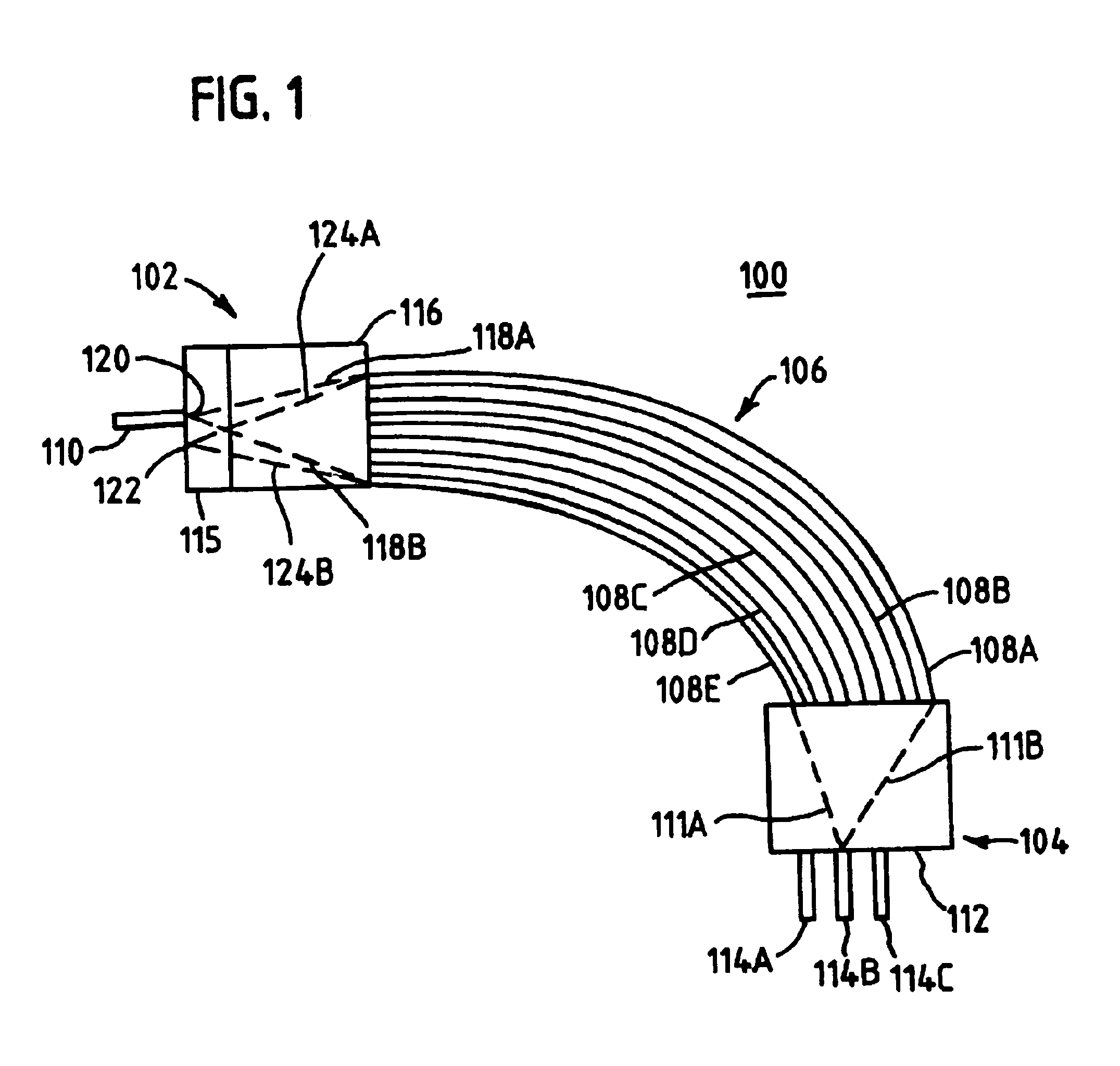
[0022]FIG. 1 illustrates a top vie...


PUM


Abstract

An arrayed waveguide grating including a waveguide array extending between two free propagation regions is disclosed. One free propagation region is coupled to an input waveguide, and the other free propagation region is coupled to output waveguides. In an example, the input-side free propagation region has two sections that are moveable relative to one another. Movement is achieved by using, for example, a thermally responsive actuator that moves the input waveguide a desired distance to compensate for a temperature change. An arm formed of a low thermal expansion coefficient metal may be used as a thermally responsive actuator moving a substrate. In another example, both the input side and the output side free propagation regions have sections moveable relative to one another and, therefore, less movement is required to correct for thermal variations. An N×N arrayed waveguide grating may also be formed.

Description

FIELD OF THE RELATED ART[0001]The present invention generally relates to arrayed waveguide gratings and, more particularly, to an apparatus for thermal compensation of an arrayed waveguide grating.BACKGROUND OF THE PRIOR ART[0002]Increasingly, optical network designers have sought to determine the effects of environmental conditions on the performance of network equipment. The results suggest that the effects are sizable.[0003]Employed in systems from local area networks (LAN) to nationwide communication networks, optical networks are a preferred way to achieve reliable, low-cost data transmission. Though designs vary depending on size, complexity and other factors, these networks are generally a complex system of interconnected optical components that perform signal input / output, switching, data processing, data analysis, and other functions.[0004]Increasingly, as networks grow in size, optical components are placed in varied locations, some with climate control many without. Unfor...

Claims


Application Information

Patent Timeline
Patent Type & Authority Patents(United States)
IPC IPC(8): G02B6/34
CPCG02B6/12014G02B6/1203G02B6/12016
Inventor JOHANNESSEN, KJETIL
Owner INTEL CORP
Why Eureka
Try Eureka