Method for detecting silicide encroachment of a gate electrode in a semiconductor arrangement

a gate electrode and gate electrode technology, applied in the field of manufacturing semiconductor devices, can solve the problems of cost saving in the manufacturing process

Active Publication Date: 2005-10-18
GLOBALFOUNDRIES US INC
View PDF12 Cites 7 Cited by
  • Summary
  • Abstract
  • Description
  • Claims
  • Application Information

AI Technical Summary

Benefits of technology

[0007]There is a need for a method of detecting the encroachment of silicide of a gate electrode in a semiconductor arrangement in a manner that assures proper detection and is production worthy.

Problems solved by technology

This creates a cost saving in the manufacturing process.

Method used


Image

  • Method for detecting silicide encroachment of a gate electrode in a semiconductor arrangement
  • Method for detecting silicide encroachment of a gate electrode in a semiconductor arrangement
  • Method for detecting silicide encroachment of a gate electrode in a semiconductor arrangement

Examples


Embodiment Construction

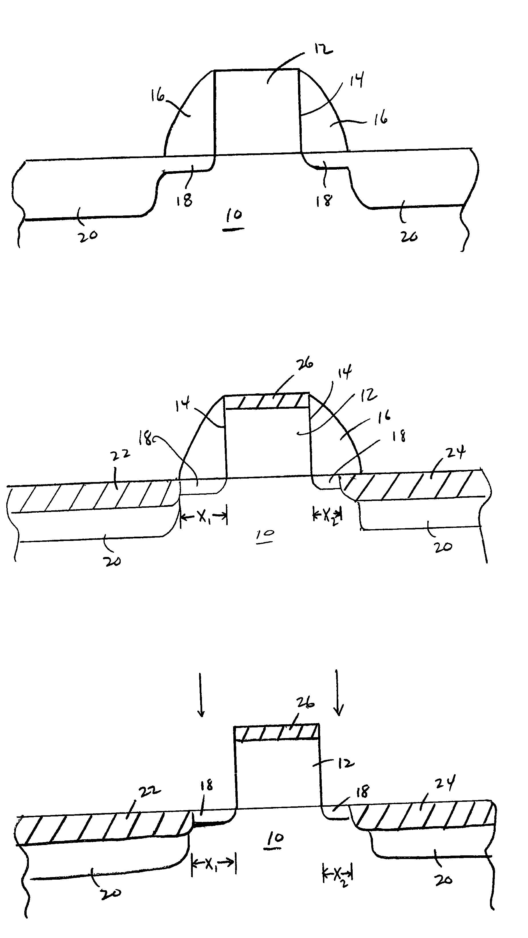
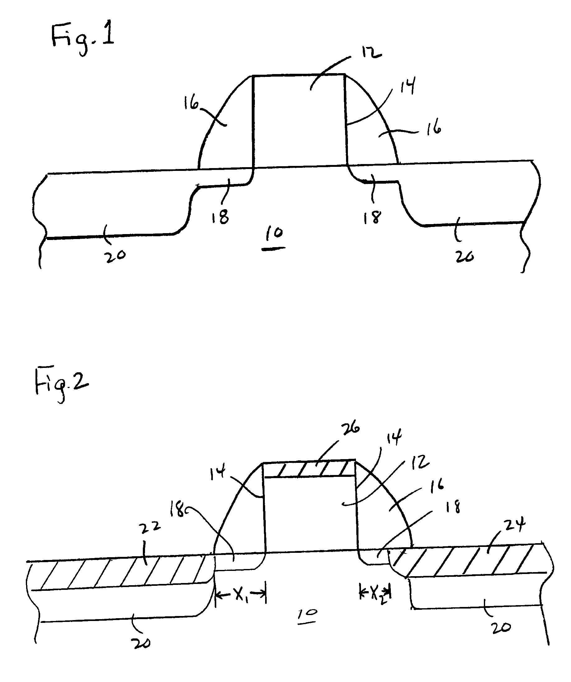
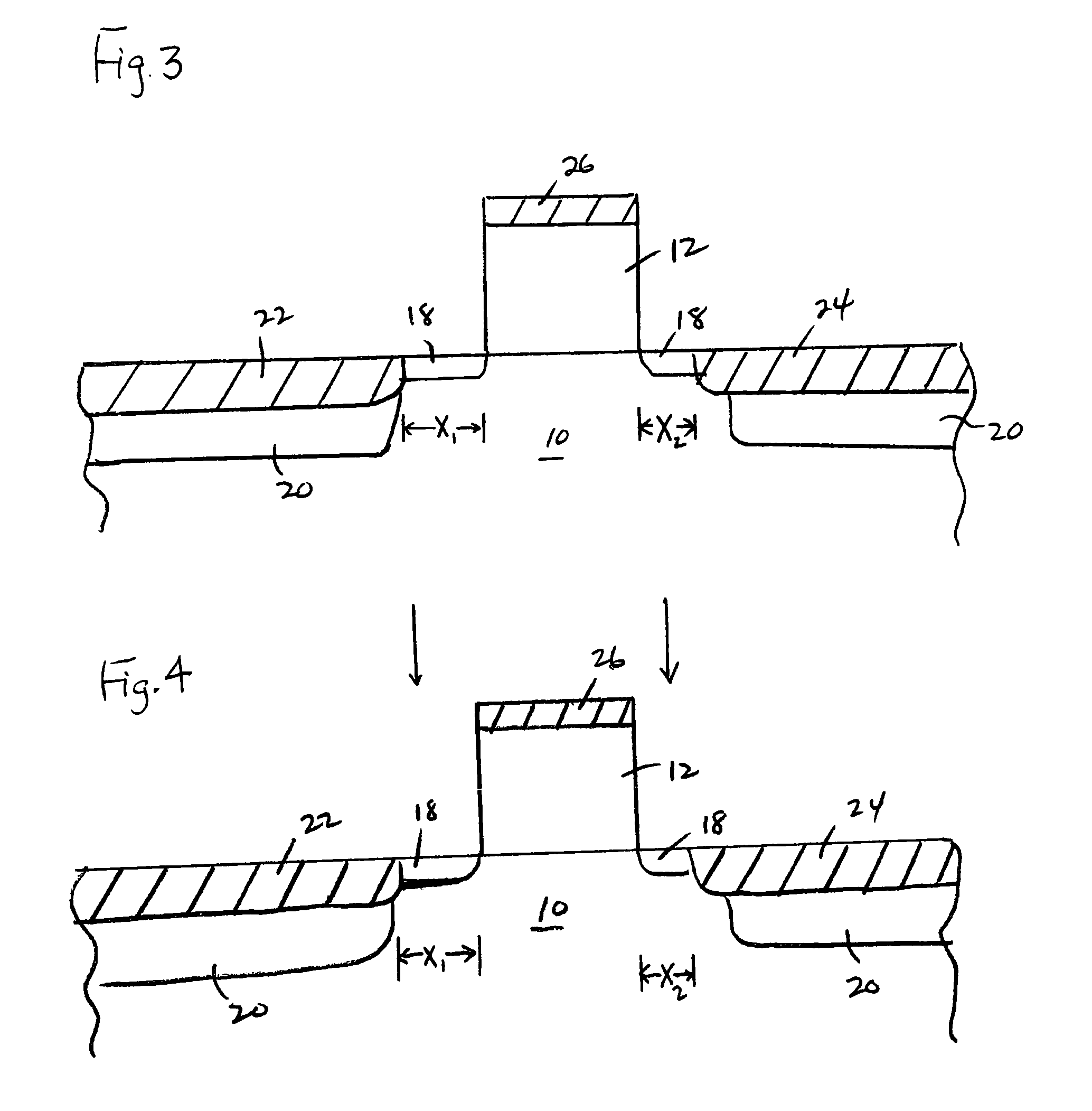
[0017]The present invention addresses and solves problems related to the detection of silicide encroachment of a gate electrode in a semiconductor arrangement, and in particular, to the obscuring of the silicide encroachment by sidewall spacers. This is achieved, at least in part, by the provision of the present invention for removal of sidewall spacers from the sidewalls of the gate electrode and from the substrate following silicide formation. This is followed by line-of-sight monitoring which can include either optical monitoring or electron microscope monitoring, for example. The observation allows for reliable detection of silicide encroachment. If the encroachment is so large that the device is unusable, further processing in the BEOL can be avoided, providing an overall cost savings.

[0018]FIG. 1 schematically depicts a cross-section of a semiconductor device during one phase of manufacturing in accordance with embodiments of the present invention. On a substrate 10, such as a...


PUM


Abstract

A method of detecting silicide encroachment to the sidewalls of a gate electrode includes forming silicide at a device, with sidewall spacers defining a desired separation of the silicide from the sidewalls of the gate electrode. After silicide formation, the sidewall spacers are removed and line-of-sight monitoring is performed of the region previously obscured by the sidewall spacers, thereby permitting detection of silicide encroachment.

Description

FIELD OF THE INVENTION[0001]The present invention relates to manufacturing semiconductor devices, and more particularly, to the formation of silicide and detection of silicide encroachment in semiconductor arrangements.BACKGROUND OF THE INVENTION[0002]As feature sizes of metal-oxide-semiconductor (MOS) and complementary metal-oxide-semiconductor (CMOS) devices are reduced into the deep sub-micron range, so-called “short-channel” effects arise which tend to limit device performance. Deep junctions, as provided in PMOS devices, and high-on resistance, are problematic for voltages less than 2V.[0003]For P-channel MOS transistors of short-channel type, the major limitation on performance arises from “punch-through” effects which occur with relatively deep junctions. In such instances, there is a wider sub-surface depletion effect and it is easier for the field lines to extend from the drain region to the source region, resulting in the above-mentioned “punch-through” current problems an...

Claims


Application Information

Patent Timeline
Patent Type & Authority Patents(United States)
IPC IPC(8): H01L21/66H01L21/336
CPCH01L22/24H01L29/7842H01L29/665H01L29/6653
Inventor BROWN, DAVID E.SUN, SEY-PING
Owner GLOBALFOUNDRIES US INC
Why Eureka
Try Eureka