Yield maximization in the manufacture of integrated circuits

a technology of integrated circuits and yield maximization, applied in the field of integrated circuits, can solve the problems of unavoidable cost, large output driver transistors with a larger delay, and complex implementation of logic functions, so as to improve the yield of fully functional ics, improve the yield of logic blocks, and improve the yield of ics.

Inactive Publication Date: 2005-10-18
ARM INC
View PDF6 Cites 198 Cited by
  • Summary
  • Abstract
  • Description
  • Claims
  • Application Information

AI Technical Summary

Benefits of technology

[0014]A first embodiment of the present invention operates to improve the yield of ICs that use standard cells to implement their logic functions. Instead of the traditional area minimization approach to improving yield of the logic blocks that allows trade-offs between area and other design specification attributes like power and performance, a set of yield enhancing variants for selected standard cells are also offered to the designer. The different yield enhancing standard cell designs are designed and characterized to compensate for a particular yield limiting factor or factors present in different semiconductor manufacturing environments for different process geometries. The synthesis tool is also modified to make use of the characterized yield data. During the synthesis of the logic functions by the tool, depending upon which parameters are given priority, different variants of the standard cell will be selected from the library, using their yield characterization data as a selection guide, to realize a design optimized to increase the yield of fully functional ICs.
[0015]In other embodiments of the present invention, other areas of the IC that typically utilize complex and specialized functions can also be implemented as yield enhancing variants by creating multiple different versions for each hard macro. For example, Input / Output (I / O) cells are typically duplicated around the IC's core and permit signal flow into and out of the core. These cells are usually hand selected by the IC designer. A set of yield enhancing variants for selected I / O cells will be offered to the designer. The designer will then be able to select among a plurality of different yield enhancing I / O cell designs, wherein each of the plurality has been designed and characterized to compensate for a particular yield limiting factor or factors that are present in different semiconductor manufacturing environments and in different process geometries. The availability of different variants of the I / O cells optimized for increased yield in different manufacturing processes will allow design of a functional IC that can be manufactured with high yield.

Problems solved by technology

Implementing logic functions is much more complex due to the typically large number of standard cells, ranging from tens of thousands to tens of millions, needed to implement the logic functions.
Although the selection of the correctly sized cell is driven by the design, it is unavoidable that a larger cell (larger output driver transistors) will have a greater delay than a smaller cell.
One optimization target for IC design is cost.
Although the described process and apparatus to create the smallest implementation of an IC incorporating the various building blocks that include logic functions and logic circuits functions reasonably well, it does not consider manufacturability as a key variable.
Until recently, die area was the primary factor affecting IC yield (usable dies per wafer) and hence IC cost.
One factor is the increased complexity of each step in process manufacturing.
For example, depending on the manufacturing processes used to fabricate the IC, different problems affecting yield can manifest themselves.
Certain IC fabrication plants have yield limiting problems with particular process technologies.
For example, one process technology may have difficulties with contact formation between metal and polysilicon and another process technology might have difficulties with formation of transistors.
Similarly, another technology or plant may have problems with metallization or diffusion formation.
In some processes, increases in the leakage currents through transistors beyond the tolerance limits of the design can be a possible yield limiter.
It has become increasingly difficult to accurately align and form each of these contacts and vias, which in turn decreases the yield of usable ICs from any given fabrication process.
Different problems may be more or less acute for a given IC when different fabrication processes at different plants are used.

Method used


Image

  • Yield maximization in the manufacture of integrated circuits
  • Yield maximization in the manufacture of integrated circuits
  • Yield maximization in the manufacture of integrated circuits

Examples


Embodiment Construction

[0021]In the following description, numerous specific details are set forth in order to provide a thorough understanding of the present invention. It will be apparent, however, to one of skill in the art that the present invention may be practiced without some or all of these specific details. In other instances, well known process steps have not been described in detail in order to unnecessarily obscure the present invention.

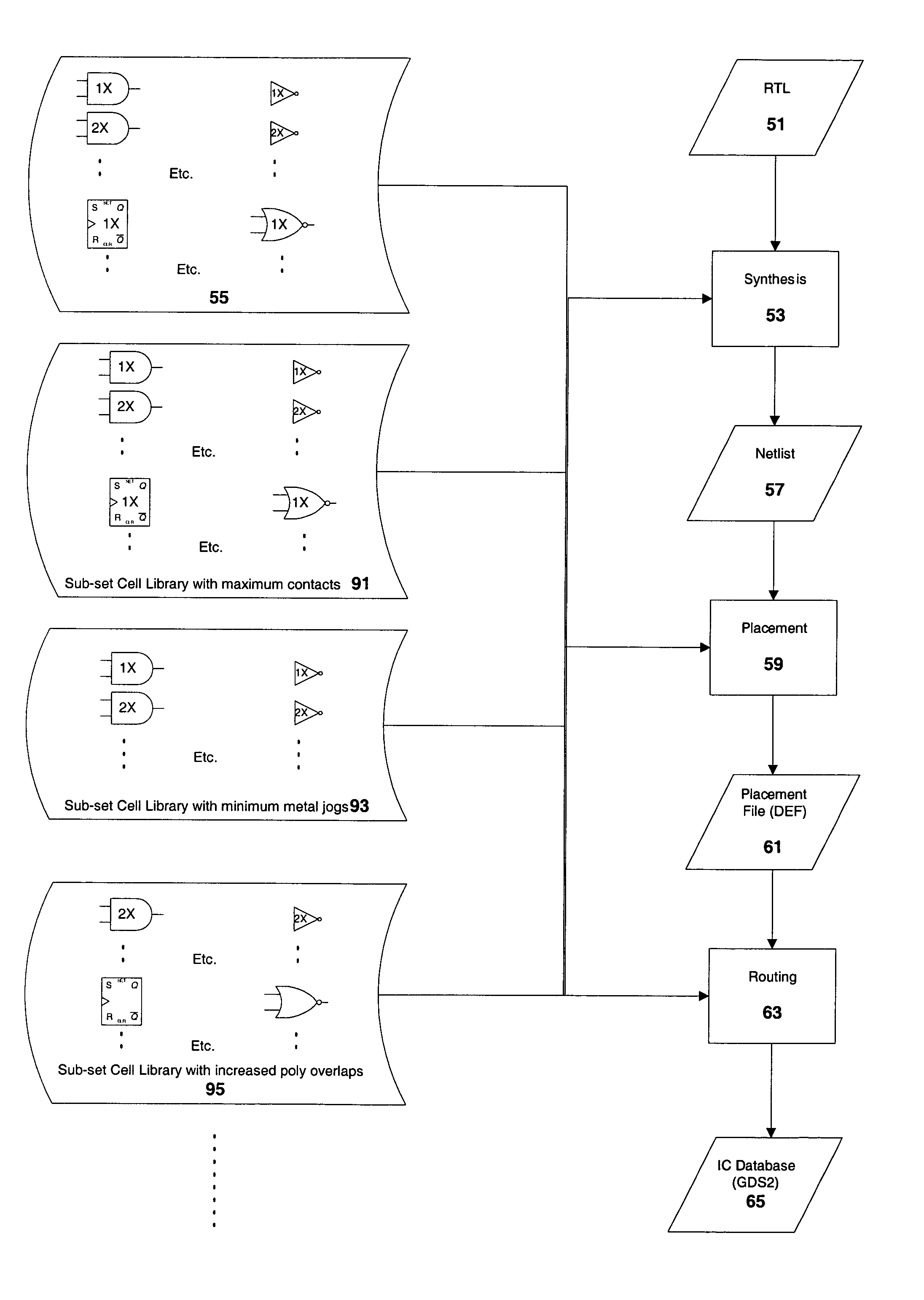
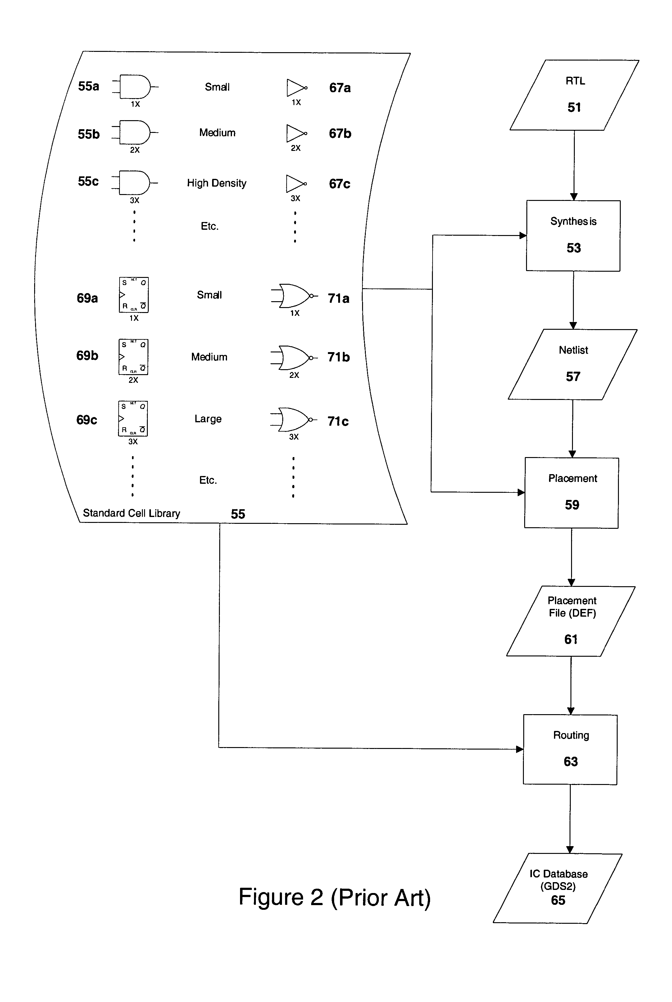
[0022]The design and manufacture of complex ICs has an established methodology and an established technology. The IC designer implements each of the functional blocks by selecting from various options to achieve the target IC specifications with minimum semiconductor area. In case of the hard macros such as memory, analog and I / Os, as well as special purpose logic blocks, each instance of these blocks is selected manually by the IC designer to achieve the desired results. For logic blocks implemented with a plurality of different standard cells, similar optimiz...


PUM


Abstract

A method and apparatus for improving the manufacturability of Integrated Circuits (ICs) formed on semiconductor dies is described. A plurality of different designs for some or all of the standard cells are made available to the circuit designer. Each different design may address a different problem associated with different manufacturing processes or a different design related yield limiter. Each of the design variants is characterized indicating its relative ease of manufacture, or it's yield sensitivity to certain IC design factors. The designer, typically with assistance from computer aided tools, can then select the standard cell variant for each of the cell used in the IC design that best addresses his or her design constraints. In other embodiments, variant versions of I / O cells and memory cells could also be created and made available to the designer in a similar fashion.

Description

BACKGROUND OF THE INVENTION[0001]1. Field of the Invention[0002]The present invention relates most generally to Integrated Circuits (ICs) formed on semiconductor substrates. More particularly, the present invention relates to methods and apparatus for improving the yield of ICs from the fabrication process.[0003]2. Description of the Related Art[0004]ICs are often implemented by connecting together different types of functional blocks to achieve the desired IC specification. As shown in FIG. 1, some of the functional blocks most often used in IC 10 are logic 12, memory 15, including RAM 13 and register files 14, Input / Output (I / O) 18, analog / mixed signal 22 and custom blocks 28. Some examples of analog / mixed signal functions are Phase Locked Loops (timing generation, de-skewing) 24 and Digital-Analog Converters (not illustrated). Of these, I / O 18, memory 15 and analog blocks 22 are typically used as a single pre-formed unit, or hard macro, by the IC designer, whereas some of the oth...

Claims


Application Information

Patent Timeline
Patent Type & Authority Patents(United States)
IPC IPC(8): G06F17/50
CPCG06F17/5045G06F30/30
Inventor TEMPLETON, MARKGANDHI, DHRUMIL
Owner ARM INC
Why Eureka
Try Eureka