SPM sensor and process for producing it
- Summary
- Abstract
- Description
- Claims
- Application Information
AI Technical Summary
Benefits of technology
Problems solved by technology
Method used
Image
Examples
Embodiment Construction
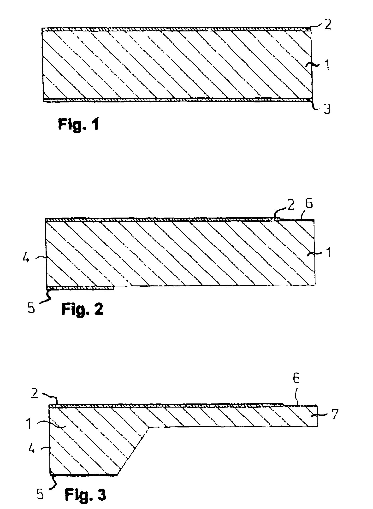
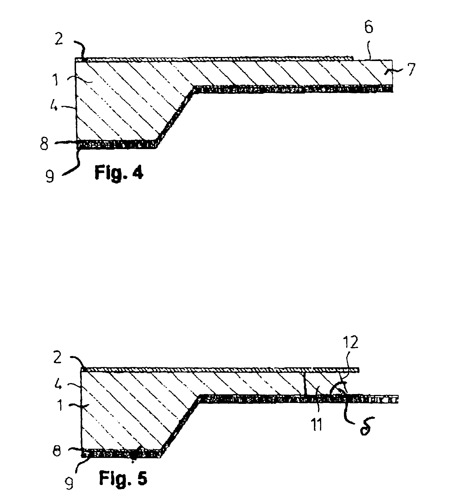
[0018]FIG. 1 shows a (100)-silicon wafer 1, in which the top side has been coated with a silicon oxide layer 2 and the underside has been coated with a silicon oxide layer 3. Next, as shown in FIG. 2, the mask for producing the holding element 4 is fabricated as a result of a photoresist being applied to the wafer underside and patterned and the photomask being transferred to the silicon oxide layer 3. The silicon oxide layer 3 on the wafer underside is in the process partially removed, so that only the region 5 for the holding element 5 remains in place. The wafer top side with the silicon oxide layer 2 is covered by a protective resist. All the photoresists which have been applied are also eliminated following the removal of the silicon oxide layer 3.
[0019]In the next step, to fabricate the mask for producing the cantilever and the cantilever tip, a photoresist is applied to the wafer top side and patterned, and the photomask is transferred to the silicon oxide. The silicon oxide ...
PUM
| Property | Measurement | Unit |
|---|---|---|
| Angle | aaaaa | aaaaa |
| Angle | aaaaa | aaaaa |
Abstract
Description
Claims
Application Information
 - R&D Engineer
- R&D Manager
- IP Professional
- Industry Leading Data Capabilities
- Powerful AI technology
- Patent DNA Extraction
Browse by: Latest US Patents, China's latest patents, Technical Efficacy Thesaurus, Application Domain, Technology Topic, Popular Technical Reports.
© 2024 PatSnap. All rights reserved.Legal|Privacy policy|Modern Slavery Act Transparency Statement|Sitemap|About US| Contact US: help@patsnap.com


