Method and apparatus of controlling a pixel reset level for reducing an image lag in a CMOS sensor

a cmos sensor and reset level technology, applied in the field of pixel reset level control, can solve the problems of high power dissipation of large arrays, ccd imagers suffer from a number of drawbacks, and ccds are also susceptible to radiation damage, so as to reduce the image lag in cmos.

Active Publication Date: 2005-10-25
TAIWAN SEMICON MFG CO LTD
View PDF14 Cites 24 Cited by
  • Summary
  • Abstract
  • Description
  • Claims
  • Application Information

AI Technical Summary

Benefits of technology

[0010]To achieve these and other advantages and in order to overcome the disadvantages of the conventional image sensor in accordance with the purpose of the invention as embodied and

Problems solved by technology

However, CCD imagers suffer from a number of drawbacks.
CCDs are also susceptible to radiation damage, require good light shielding to avoid smear and have high power dissipation for large arrays.
Other types of imager devices have problems as well.
Photodiode a

Method used


Image

  • Method and apparatus of controlling a pixel reset level for reducing an image lag in a CMOS sensor
  • Method and apparatus of controlling a pixel reset level for reducing an image lag in a CMOS sensor
  • Method and apparatus of controlling a pixel reset level for reducing an image lag in a CMOS sensor

Examples


Embodiment Construction

[0024]Reference will now be made in detail to the preferred embodiments of the present invention, examples of which are illustrated in the accompanying drawings. Wherever possible, the same reference numbers are used in the drawings and the description to refer to the same or like parts.

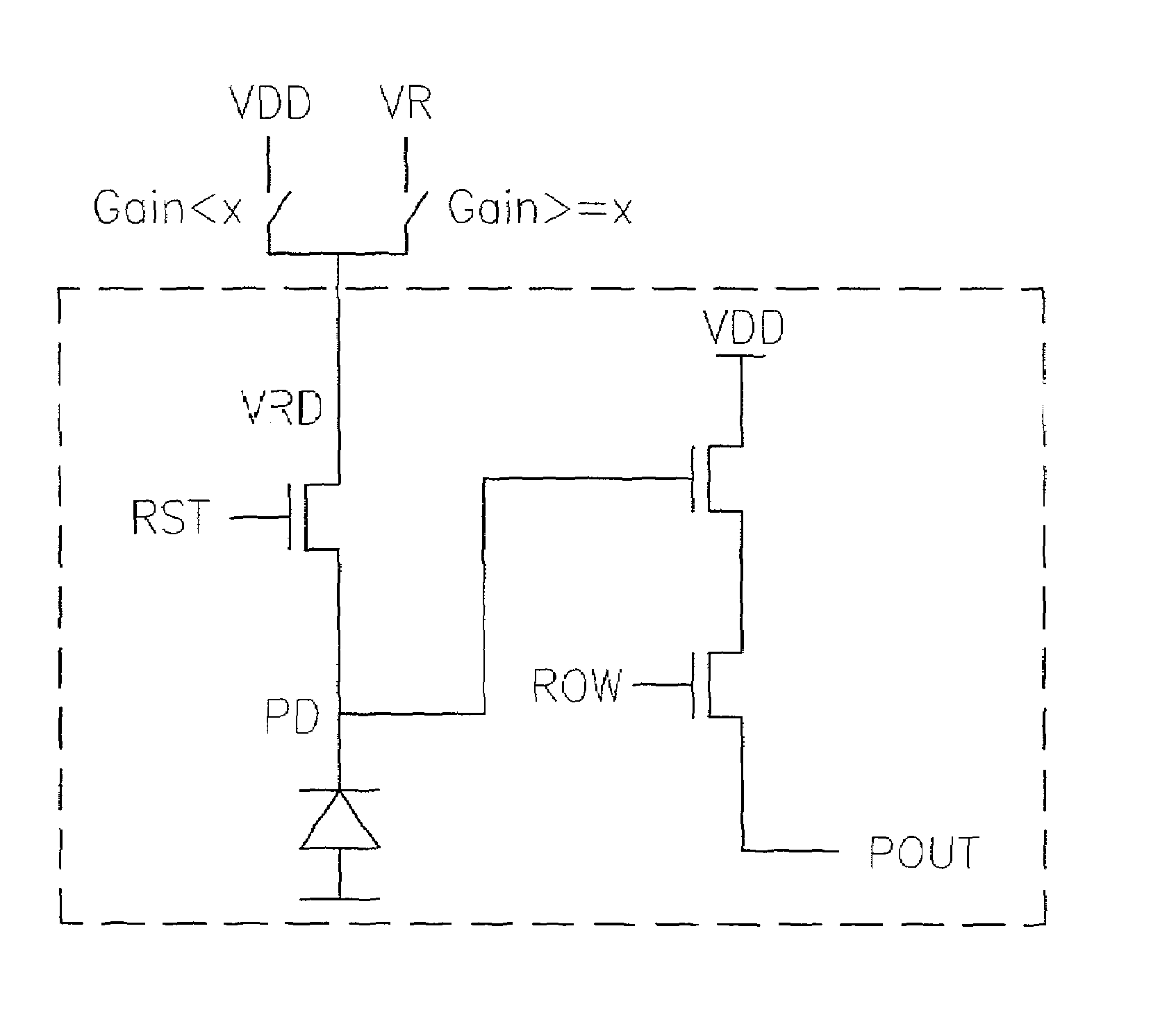
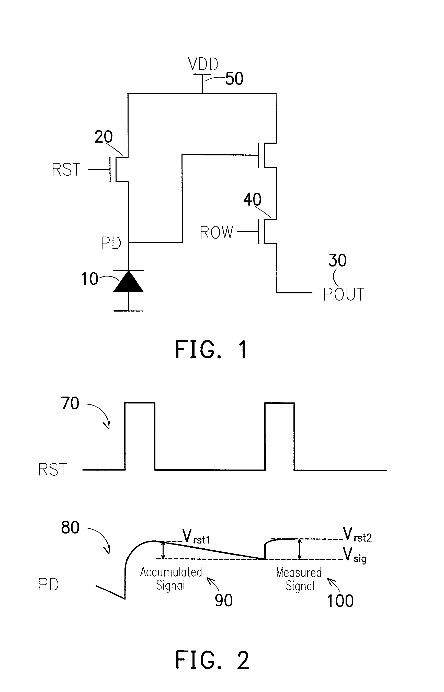
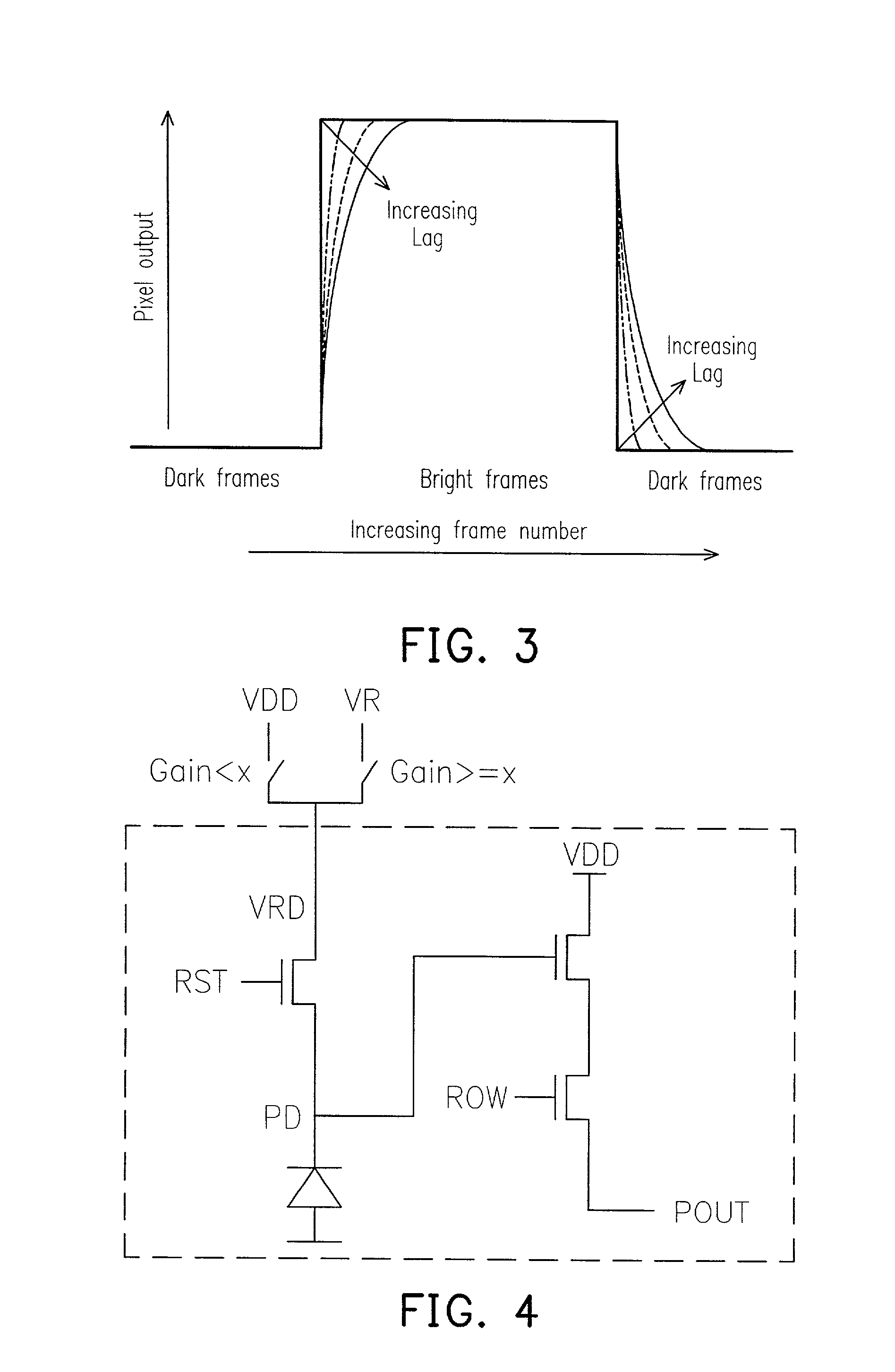
[0025]Refer to FIG. 1, which is a circuit diagram illustrating a CMOS photodiode pixel. A CMOS image sensor pixel consists of an imaging device such as a photodiode (PD) 10, a reset transistor 20, a readout transistor 30 and a selection transistor 40. All of the transistors are of the same type, for example n-channel, due to area limitations. The drains of the readout and reset transistors are connected to the positive supply (VDD) 50.

[0026]The operation of the image sensor is as follows. Signal charge integration begins when PD 10 is reset (to Vrst1) by pulsing the reset gate (RST) 20 high. During charge integration, photo-generated electrons are accumulated on the photodiode 10, making the PD volta...


PUM


Abstract

The invention provides a method and apparatus for reducing image lag in CMOS active pixel sensors at low light levels by controlling the reset level. By ensuring that the reset level is independent of the preceding signal level, the problem of image lag can be avoided. Always resetting a photodiode to a fixed voltage is a hard reset. The maximum signal swing is limited by the reset level and the column readout amplifier. If the column circuits are not modified, using hard reset can reduce the maximum signal swing. However in dark images only a portion of the full scale is used. Therefore the amplifier gain setting can be used to determine whether to use a hard reset or soft reset. This method and apparatus for using hard or soft reset dependent on signal level improves image quality at low light levels without compromising performance at high illumination.

Description

CROSS-REFERENCE TO RELATED APPLICATION[0001]This application claims the priority benefit of U.S Provisional Application Ser. No. 60 / 217,534, filed Jul. 12, 2000.BACKGROUND OF THE INVENTION[0002]1. Field of Invention[0003]The present invention relates to a pixel reset level control, and more particularly, to reducing image lag in CMOS active pixel sensors at low light levels by controlling the reset level.[0004]2. Description of Related Art[0005]Image acquisition can be achieved by various semiconductors. Some of the conventional devices are charge-coupled devices (CCDs), photodiode arrays, charge injection devices and hybrid focal plane arrays. Of these CCDs are frequently implemented, due to the fact that they represent a mature technology, are capable of large formats and very small pixel size and they facilitate noise-reduced charge domain processing techniques such as binning and time delay integration.[0006]However, CCD imagers suffer from a number of drawbacks. For example, th...

Claims


Application Information

Patent Timeline
IPC IPC(8): H04N3/15H04N5/363H04N5/374H04N9/07
CPCH04N5/361H04N5/3741H04N5/376H04N25/63H04N25/766H04N25/74
Inventor MENDIS, SUNETRA K.SHU, TZI-HSIUNG
Owner TAIWAN SEMICON MFG CO LTD
Why Eureka
Try Eureka