Semiconductor device simulation method, semiconductor device and fabrication method thereof, circuit board, electro-optical apparatus, and electronic device

a semiconductor and simulation method technology, applied in the field of semiconductor device simulation method, can solve the problems of not being able to use the above-described electron and positive-hole carrier continuity equation

Inactive Publication Date: 2005-10-25
SEIKO EPSON CORP
View PDF7 Cites 7 Cited by
  • Summary
  • Abstract
  • Description
  • Claims
  • Application Information

AI Technical Summary

Benefits of technology

[0032]Therefore, an object of the present invention is to obtain an accurate and high-precision semiconductor device simulation method that is directed toward an organic thin film transistor that employs an organic semiconductor in which mobility is highly dependent on field strength.

Problems solved by technology

In other words, in cases where an electric field is present, when the physicality of the semiconductor is not isotropic, the above-described Einstein relation is not established, and hence it is not possible to use the above-described electron and positive-hole carrier continuity equations.

Method used


Image

  • Semiconductor device simulation method, semiconductor device and fabrication method thereof, circuit board, electro-optical apparatus, and electronic device
  • Semiconductor device simulation method, semiconductor device and fabrication method thereof, circuit board, electro-optical apparatus, and electronic device
  • Semiconductor device simulation method, semiconductor device and fabrication method thereof, circuit board, electro-optical apparatus, and electronic device

Examples


Embodiment Construction

[0058]Preferred embodiments of the present invention will be described below, but the following embodiments do not limit the inventions according to the scope of the claims, and all the combinations of characteristics described in these embodiments are not required by the resolving means of the invention.

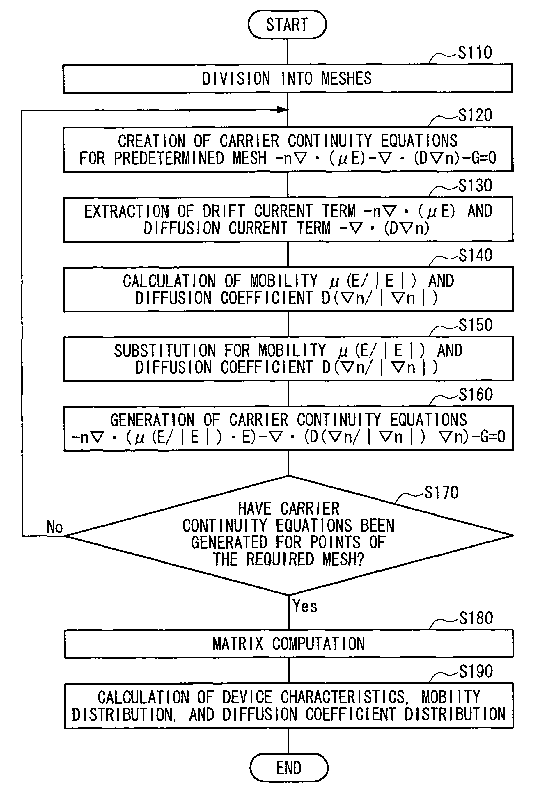
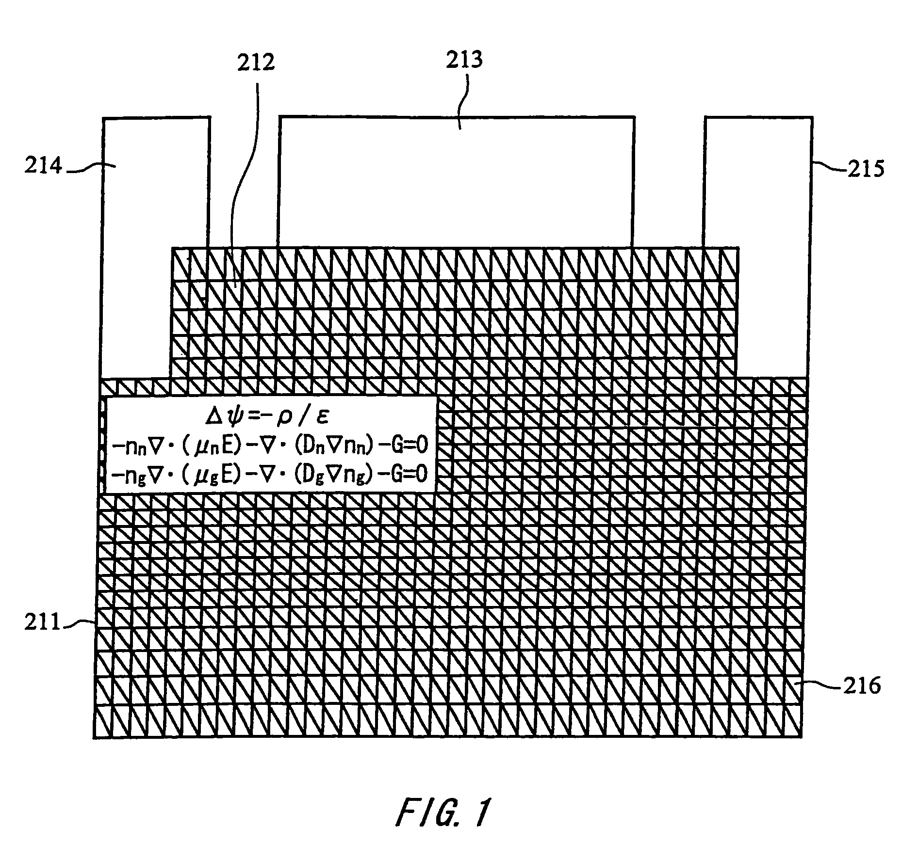
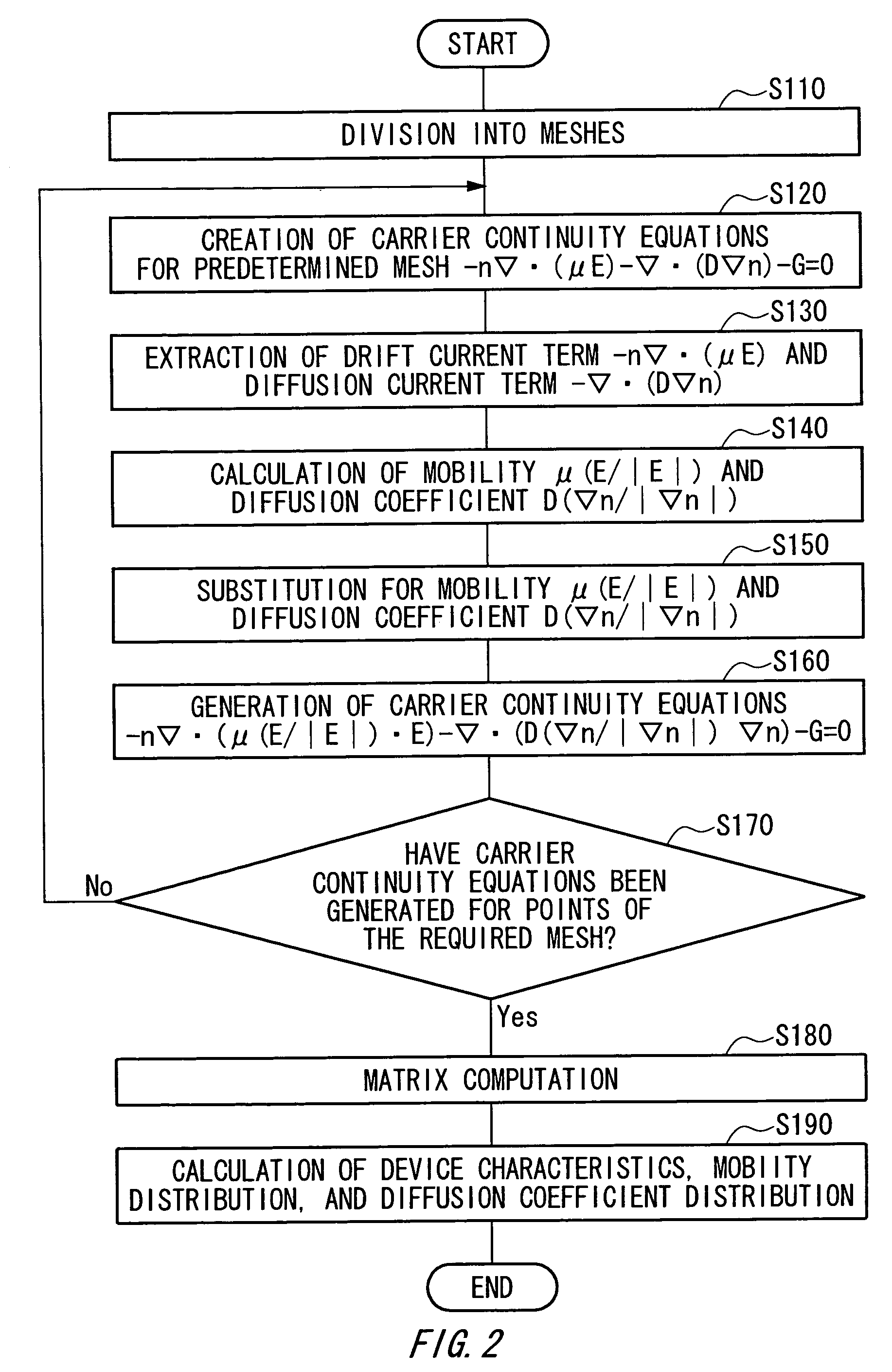
[0059]FIG. 1 shows a semiconductor device simulation method according to a first embodiment of the present invention, and FIG. 2 is a flowchart for the semiconductor device simulation method according to this embodiment. The semiconductor device simulation method according to this embodiment will now be described using an organic thin film transistor as an example of a semiconductor device. The organic thin film transistor in this example is constituted comprising an organic semiconductor 211; an insulation film 212 formed on the surface of the organic semiconductor 211; a gate electrode 213 formed on the insulation film 212; and a source electrode 214 and drain electrode 215 which ...


PUM

PropertyMeasurementUnit
semiconductor device simulationaaaaaaaaaa
electric fieldaaaaaaaaaa
carrier densityaaaaaaaaaa

Abstract

The present invention provides an accurate and high-precision semiconductor device simulation method that is directed toward an electronic device whose physicality is not isotropic because the mobility of an organic thin film transistor, that employs an organic semiconductor, and the like, is highly dependent on field strength. In a semiconductor device simulation method which divides a semiconductor device of a two-dimensional structure or three-dimensional structure into meshes, and solves physical equations such as a potential equation and a carrier transport equation, for the meshes, a drift current resulting from an electric field and a diffusion current caused by a carrier density gradient are handled separately.

Description

BACKGROUND OF THE INVENTION[0001]1. Field of the Invention[0002]The present invention relates to a semiconductor device simulation method, and more particularly to an accurate and high-precision semiconductor device simulation method that is directed toward organic thin film transistors, a semiconductor device and fabrication method thereof, and a circuit board, electro-optical apparatus and electronic apparatus.[0003]2. Description of the Related Art[0004]Semiconductor device simulation involves predicting the characteristics of semiconductor devices from the structure and material properties, and so forth, of semiconductor devices or analyzing the operation of such devices. Objects of this simulation are an improvement in development efficiency by means of a decrease in the number of manufacturing experiments, the implementation of the optimum design by means of a comparison of a multiplicity of characteristics, and the proposal of development guidelines through estimation of the ...

Claims


Application Information

Patent Timeline
Patent Type & Authority Patents(United States)
IPC IPC(8): G06F17/50G02F1/1368H01L29/786
CPCG06F17/5018G06F30/23
Inventor KIMURA, MUTSUMI
Owner SEIKO EPSON CORP
Why Eureka
Try Eureka