
Integrated circuit packaging for improving effective chip-bonding area

a technology of integrated circuits and integrated circuits, applied in the direction of adhesives, electrical apparatus, semiconductor devices, etc., can solve the problem of easy to occur popcorn defects, and achieve the effect of excellent reliability, and improving effective chip bonding area

Active Publication Date: 2005-11-01
CHIPMOS TECH INC
View PDF9 Cites 7 Cited by
  • Summary
  • Abstract
  • Description
  • Claims
  • Application Information

AI Technical Summary

Benefits of technology

[0004]In accordance with a first aspect of the invention there is provided a process for making an integrated circuit package comprising the steps of: providing a substrate having a chip-attaching surface; applying an A-stage liquid paste on the chip-attaching surface of the substrate, the A-stage liquid paste including a thermosetting material and a solvent; heating the substrate to remove the solvent of the A-stage liquid paste in a manner that the A-stage liquid paste is transformed into a dry B-stage film layer; attaching a chip to the chip-attaching surface of the substrate by the B-stage film layer, the B-stage film layer being maintained in a partially cured condition; electrically connecting the chip with the substrate having the B-stage film layer; and forming a molding compound on the chip-attaching surface of the substrate, the packing pressure for the molding compound being larger than the chip-attaching pressure in a manner that the partially-cured B-stage film layer re-bonds the chip to improve effective chip-bonding area.
[0005]As the packing pressure for the molding compound is larger than the chip-attaching pressure, the B-stage film layer can further closely re-bond the chip for improving effective chip-bonding area in molding step.
[0007]As the B-stage film layer has a glass transition temperature (Tg) lower than chip-attaching temperature and has a thermosetting temperature lower than thermosetting temperature of the molding compound, the B-stage film layer can be closely compressed between the chip and the substrate to remove gaps or voids in the molding step.
[0008]The packing pressure for the molding compound is preferably approximately 6.9 MPa (1000 psi) to 10.3 MPa (1500 psi), which is larger than the chip-attaching pressure, so that the B-stage film layer can be closely compressed to re-bond the chip in order to improve the effective chip-bonding area. The heating temperature in the molding step is preferably approximately 150° C. to 200° C., which is higher than the fully curing temperature of the B-stage film layer, so as to cure the B-stage film layer and the molding compound simultaneously.

Problems solved by technology

A popcorn defect is easy to happen while executing reliability test such as moisture or burn-in test after packaging.

Method used


Image

  • Integrated circuit packaging for improving effective chip-bonding area
  • Integrated circuit packaging for improving effective chip-bonding area
  • Integrated circuit packaging for improving effective chip-bonding area

Examples


Embodiment Construction

[0015]Referring to the drawings attached, the present invention will be described by means of the embodiments below.

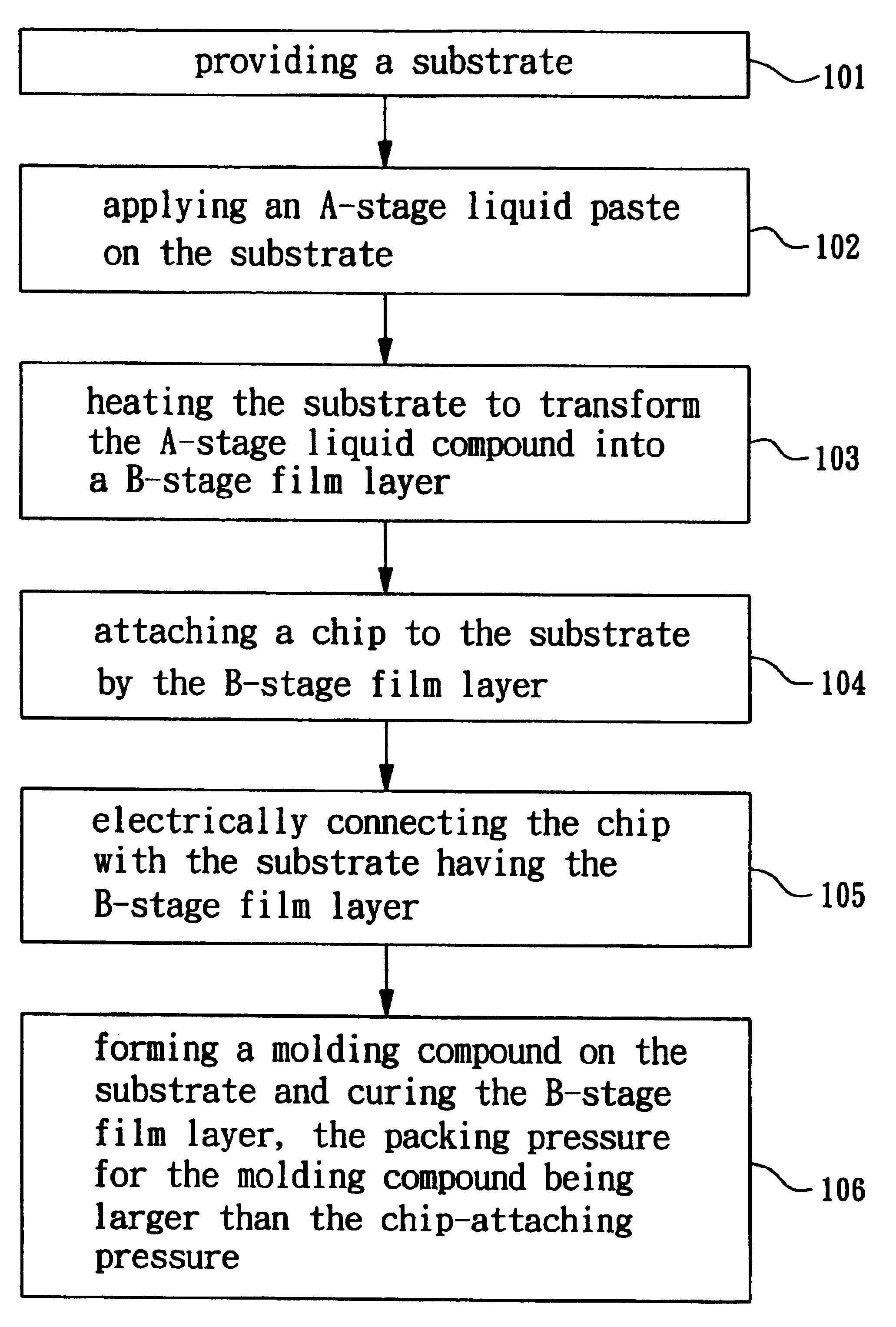
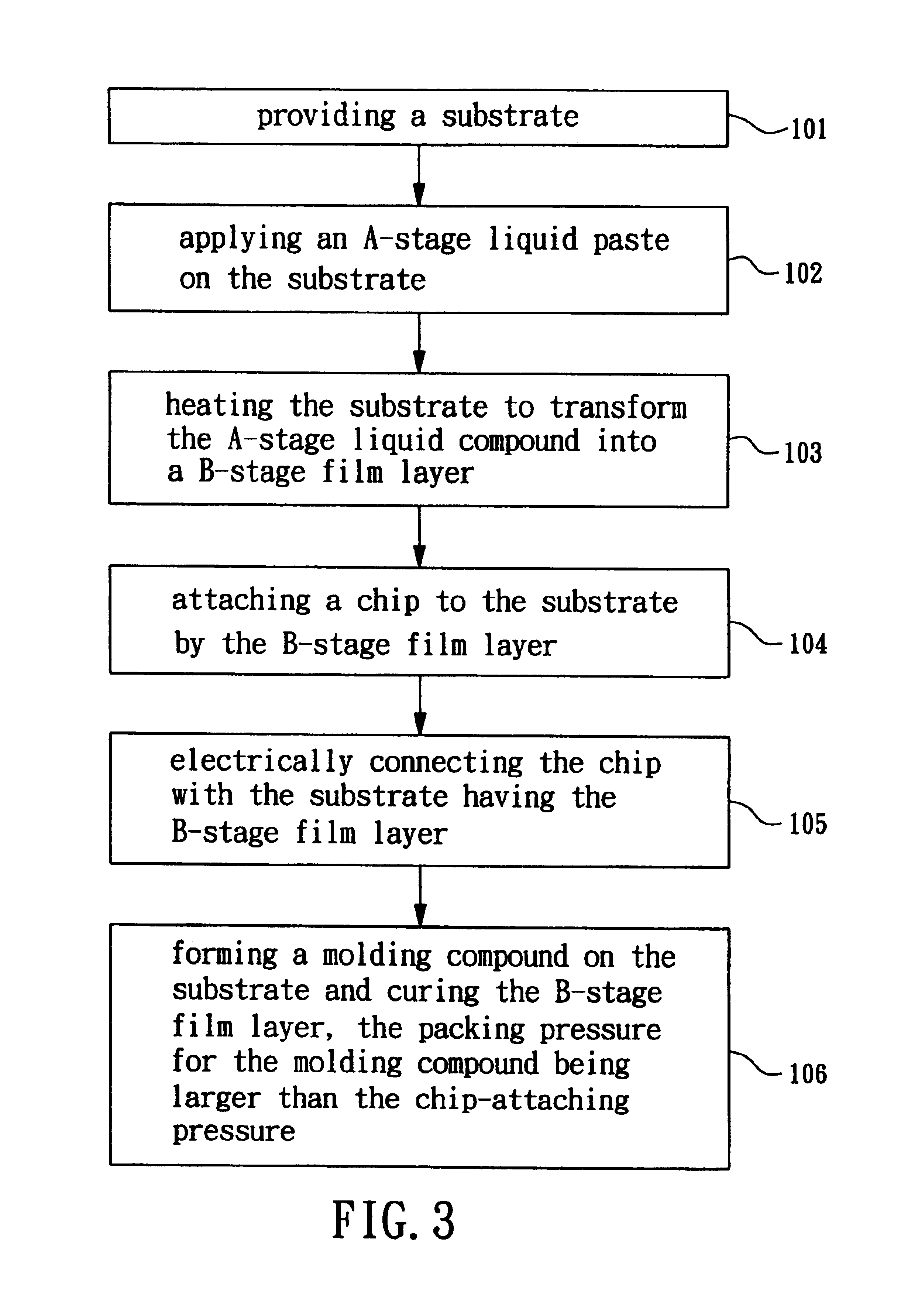
[0016]According to an embodiment of the present invention, the packaging process for improving effective chip-bonding area comprises the steps as showed in FIG. 3.

[0017]As showed in FIG. 3 and FIG. 4A, the first step 101 is to provide a substrate 110, the substrate 110 is a high density wiring substrate for integrated circuit package, such as BT printed circuit board, thin film wiring board or TAB tape. The substrate 110 has a chip-attaching surface 111, and a plurality of connect pads 112 (or fingers) are formed on the chip-attaching surface 111 for electrically connecting with the chip 130. But the location of the connect pads 112 is not limited, the connect pads 112 can be formed on the other surface of the substrate 110 in another instance. Advantageously, the other surface of the substrate 110 corresponding to the chip-attaching surface 111 is a surface-mounting s...


PUM

PropertyMeasurementUnit
packing pressureaaaaaaaaaa
Tgaaaaaaaaaa
packing pressureaaaaaaaaaa

Abstract

A packaging process for improving effective chip-bonding area is disclosed in the present invention. An A-stage liquid paste is formed on a substrate and partially cured to become a B-stage film layer. The B-stage film layer is maintained without fully cured passing through a chip-attaching step and an electrically connecting step. During the molding step, the packing pressure for the molding compound (1000 psi˜1500 psi) is larger than the chip attaching pressure for enabling the B-stage film layer to be closely compressed in order to improve effective chip-bonding area. The B-stage film layer and the molding compound are cured simultaneous in the molding step.

Description

FIELD OF THE INVENTION[0001]The present invention is relating to a process for making an integrated circuit package, particularly to a process for making an integrated circuit package for improving effective chip-bonding area using a B-stage film layer as a chip bond material.BACKGROUND OF THE INVENTION[0002]It is conventional technique to utilize B-stage compound to be a chip bond material, as disclosed in R.O.C. Taiwan Patent No. 455,970 entitled “multi-chip stacked package”. The conventional B-stage compound is used for adhering two chips, it won't produce a stress between the two chips because the two chips have a same thermal coefficient. Also the B-stage compound is sealed inside the molding compound, so that the adhesive strength of the B-stage compound is not demanded severely.[0003]When a B-stage compound is directly configured to adhere a chip to a substrate in integrated circuit package. As showed in FIG. 1, at first a B-stage compound 13 is applied to the chip-attaching ...

Claims


Application Information

Patent Timeline
Patent Type & Authority Patents(United States)
IPC IPC(8): C09J7/00H01L21/56H01L21/02H01L21/58
CPCH01L21/565H01L24/83H01L24/32H01L24/29H01L2224/92147H01L2224/32013H01L2924/014H01L2924/01006H01L2924/15311H01L2924/14H01L2924/07802H01L2924/01079H01L2924/01075H01L2924/01059H01L2924/01057H01L2924/01033H01L2924/01005H01L2224/92247H01L2224/83885H01L2224/83856H01L2224/83194H01L2224/83192H01L2224/73265H01L2224/73215H01L2224/4824H01L2224/48227H01L2224/48091H01L2224/32225H01L2924/00014H01L2924/00012H01L2924/00H01L2924/181H01L24/73
Inventor LIN, CHUNG-HUNGCHUNG, CHO-LIANGHUANG, MING-LIANGHUANG, JESSE
Owner CHIPMOS TECH INC
Learn More