System for providing an open-cavity low profile encapsulated semiconductor package

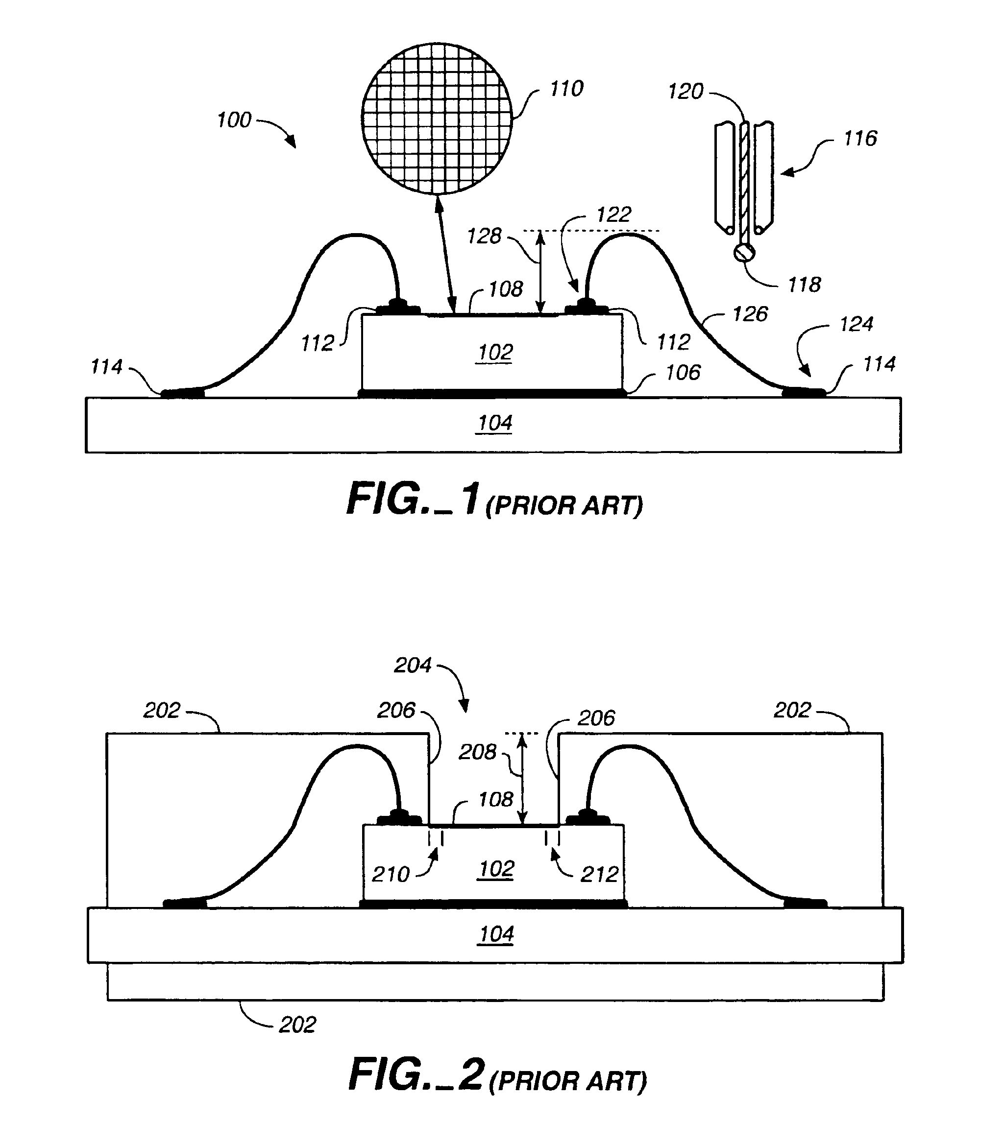
a semiconductor and low-profile technology, applied in the field of semiconductor devices, can solve the problems of package size, sensor performance degradation, and the inability to reach the portion of the sensor surface 108 by a person's finger, and achieve the effect of reducing the height of the encapsulation, reducing the height of the wire loop, and reducing the height of the pedestal

Inactive Publication Date: 2005-11-08
SOCIONEXT INC
View PDF17 Cites 126 Cited by
  • Summary
  • Abstract
  • Description
  • Claims
  • Application Information

AI Technical Summary

Benefits of technology

[0014]The present invention includes a system for wire bonding a finger sensor die to an external circuit to provide maximum access to the finger sensor surface while providing the smallest possible size to allow the device to be used in a variety of portable applications. The system reduces the height of wire loops formed by bonding wires so that the pedestal height of the encapsulation is reduced. The reduced height of the pedestal provides greater access to the sensor s...

Problems solved by technology

Unfortunately, as a result of the pedestal height, portions of the sensor surface 108 may not be reachable by a person's finger.
However, due to the effects of the pedestal height, portions of the sensor grid are unreachable, and so, the performance of the sensor may be degraded.
Another problem associated with convention fingerprint sensors is the package size.
This results in a very large package that may be unsuitable for use in portable applications.
However, due to the geometry of the die, it may ...

Method used


Image

  • System for providing an open-cavity low profile encapsulated semiconductor package
  • System for providing an open-cavity low profile encapsulated semiconductor package
  • System for providing an open-cavity low profile encapsulated semiconductor package

Examples


Embodiment Construction

[0033]The present invention includes a system for bonding wires to a finger sensor die to provide maximum access to a finger sensor surface while providing the smallest possible size. The system reduces the height of wire loops formed by bonding wires so that the pedestal height of the encapsulation material is reduced. Thus, various embodiments of the system included in the present invention are discussed in detail in the following text.

Exemplary Embodiment

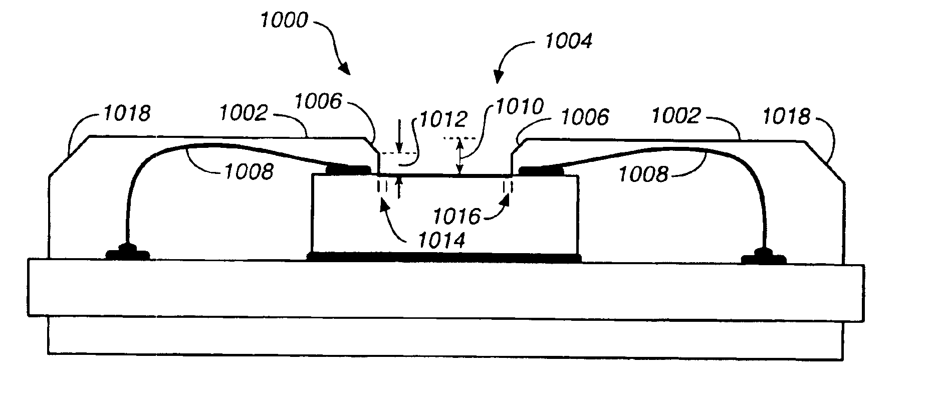
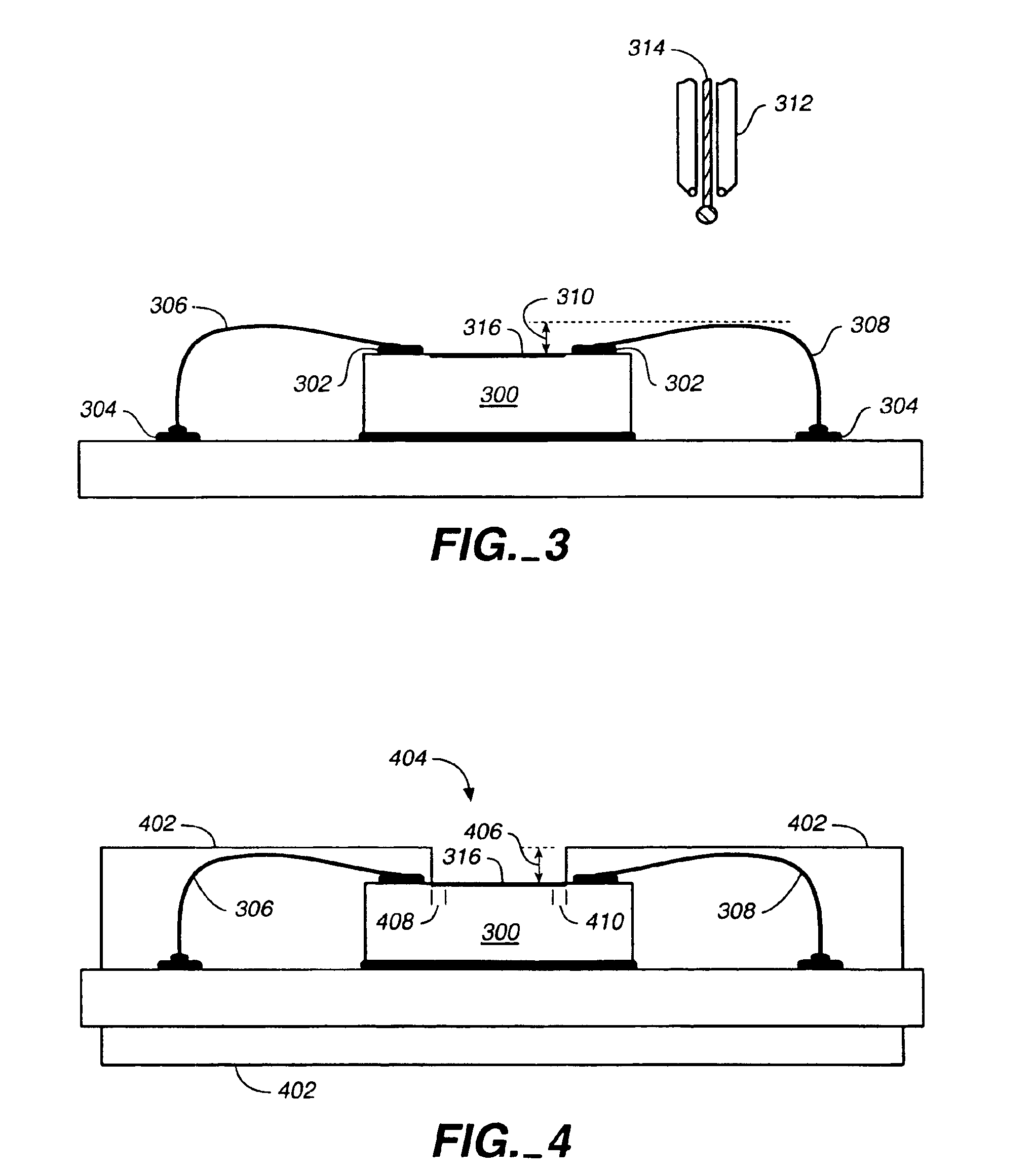
[0034]FIG. 3 shows one embodiment of a finger sensor die 300 with wires bonded between die contacts 302 and substrate contacts 304 in accordance with the present invention. Bonding wires 306, 308 are shown having very low loop heights 310 in accordance with the present invention.

[0035]To form the wire bonds as shown in FIG. 3, the capillary device 312 forms a ball at the end of a bonding wire 314 and this ball is welded to one of the substrate contacts 304. The wire 314 is then extended to a die contact where a stitch weld is cre...


PUM

PropertyMeasurementUnit
Lengthaaaaaaaaaa
Lengthaaaaaaaaaa
Electrical inductanceaaaaaaaaaa

Abstract

System for providing an open-cavity semiconductor package. The system includes a method for wire bonding a finger sensor die to an external circuit. The finger sensor die includes a sensor array having one or more die contacts that are wire bonded to one or more external contacts of the external circuit so that a usable portion of the sensor array is maximized. The method comprises steps of forming a ball at a first end of a bonding wire, forming an electrically conductive connection between the ball and a selected external contact of the external circuit, extending the bonding wire to a selected die contact so as to form a wire loop having a low loop height, and forming an electrically conductive stitch connection between a second end of the bonding wire and the selected die contact.

Description

[0001]This application claims priority under 35 U.S.C. §§ 120 and 121 as a division of U.S. patent application Ser. No. 10 / 094,954, filed Mar. 9, 2002, now U.S. Pat. No. 6,653,723.FIELD OF THE INVENTION[0002]The present invention relates to semiconductor devices, and more particularly, to a system for providing a fingerprint sensor with increased sensor accessibility.BACKGROUND OF THE INVENTION[0003]Semiconductor devices are increasingly being used as input devices for digital systems. For example, in identification and security applications, semiconductor devices are used to provide user identification information. One such device is a semiconductor fingerprint sensor.[0004]FIG. 1 shows a portion of a typical semiconductor fingerprint sensor 100. Generally, such a sensor is provided as an integrated circuit (IC). The sensor 100 includes a die (or wafer) 102 attached to a substrate 104 via an adhesive or epoxy bond 106. A sensor surface 108 of the die 102 has a conductive grid, show...

Claims


Application Information

Patent Timeline
IPC IPC(8): G06K9/00A61B5/117H01L21/60H01L23/28
CPCG06K9/0002H01L24/85H01L24/45H01L24/78H01L2224/45124H01L2224/45144H01L2224/48091H01L2224/48225H01L2224/48227H01L2224/48465H01L2224/48471H01L2224/48479H01L2224/73265H01L2224/78301H01L2224/85051H01L2224/85186H01L2224/85986H01L2924/01004H01L2924/01006H01L2924/01013H01L2924/01015H01L2924/01033H01L2924/01047H01L2924/01079H01L2924/01082H01L2924/01327H01L2924/14H01L2924/1815H01L2924/30105H01L2924/01005Y10T29/49146Y10T29/49171Y10T29/49144Y10T29/49176Y10T29/49179H01L2924/00014H01L2924/00H01L2224/85205H01L2224/85207H01L2924/181H01L2224/8592H01L24/48H01L2224/85045H01L2224/32225G06V40/1306H01L2924/00015H01L2924/00012H01L2224/4554H01L21/60
Inventor MANANSALA, MICHAEL
Owner SOCIONEXT INC
Why Eureka
Try Eureka