Interfacial trap layer to improve carrier injection

a carrier injection and facial trap technology, applied in the field of facial trap layer to improve the carrier injection, can solve the problems of large imbalance in the number of electrons and holes, low display efficiency, and inability to use the combination of electrodes and the emissive layer

Inactive Publication Date: 2005-11-08
DOLYA HOLDCO 5 LTD
View PDF5 Cites 20 Cited by
  • Summary
  • Abstract
  • Description
  • Claims
  • Application Information

AI Technical Summary

Problems solved by technology

However, if the energy barrier between the anode and the emissive layer is large enough to substantially inhibit hole injection into the emissive layer, or the energy barrier between the cathode and the emissive layer is large enough to substantially inhibit electron injection into the emissive layer, then there will be a large imbalance in the number of electrons and holes and this will lead to very few if any recombinations in the emissive layer resulting in very low display efficiency making unusable this combination of electrodes and the emissive layer.
By requiring that the energy levels match, the choice of electrodes that can be used with a certain emissive layer is limited.
In order to efficiently inject electrons into these, we would need to use very low work function metals, but these metals are highly reactive and thus very unstable.

Method used


Image

  • Interfacial trap layer to improve carrier injection
  • Interfacial trap layer to improve carrier injection
  • Interfacial trap layer to improve carrier injection

Examples


Embodiment Construction

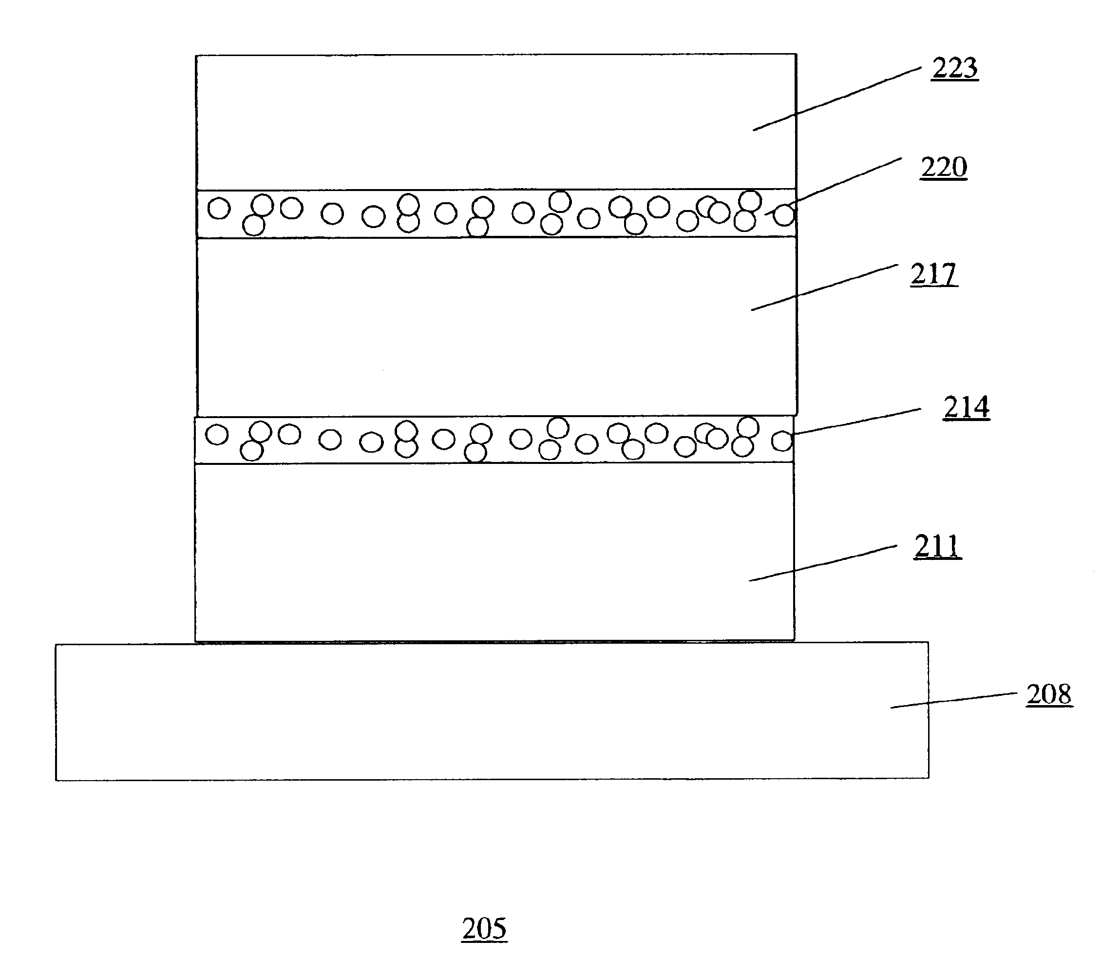
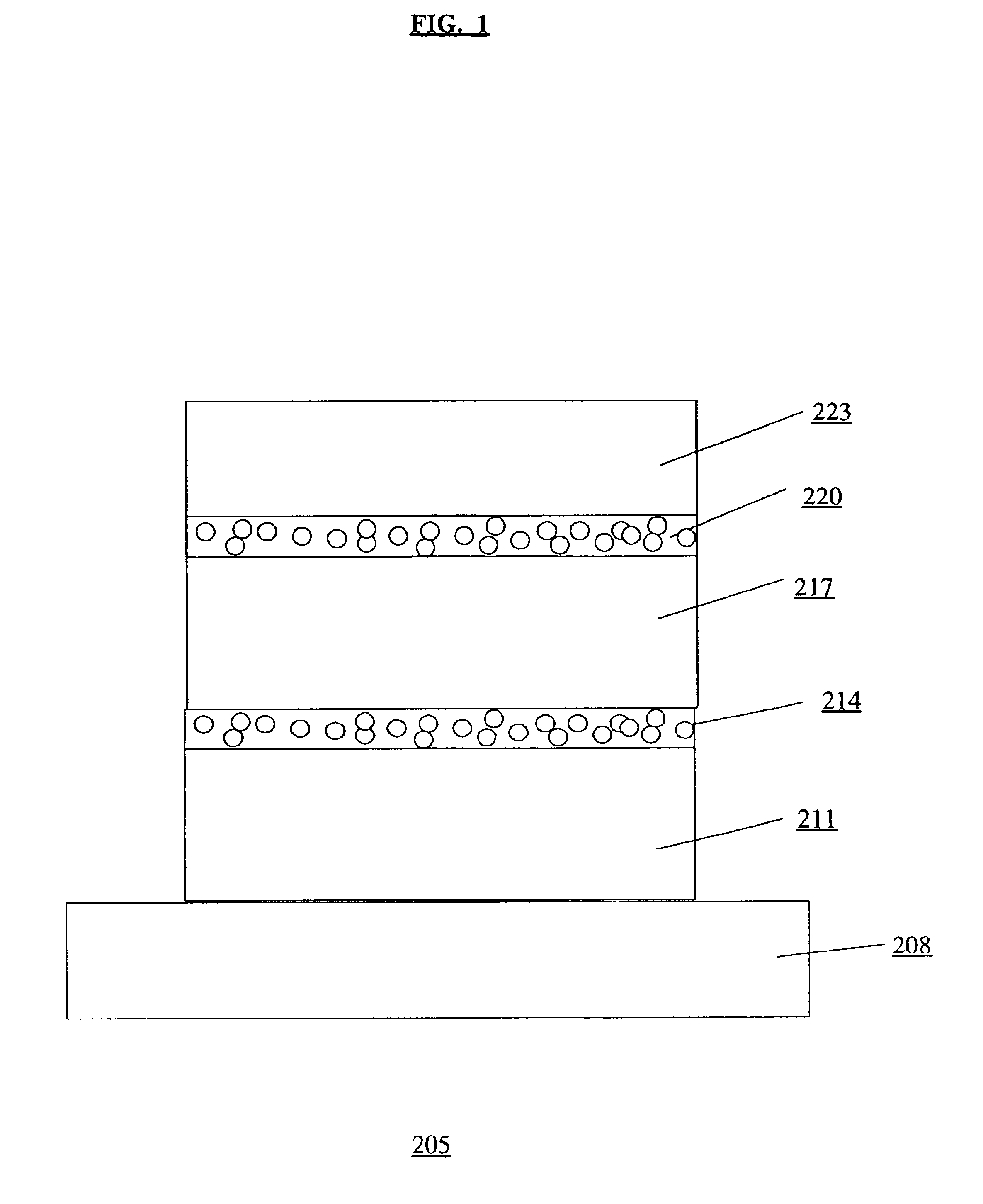
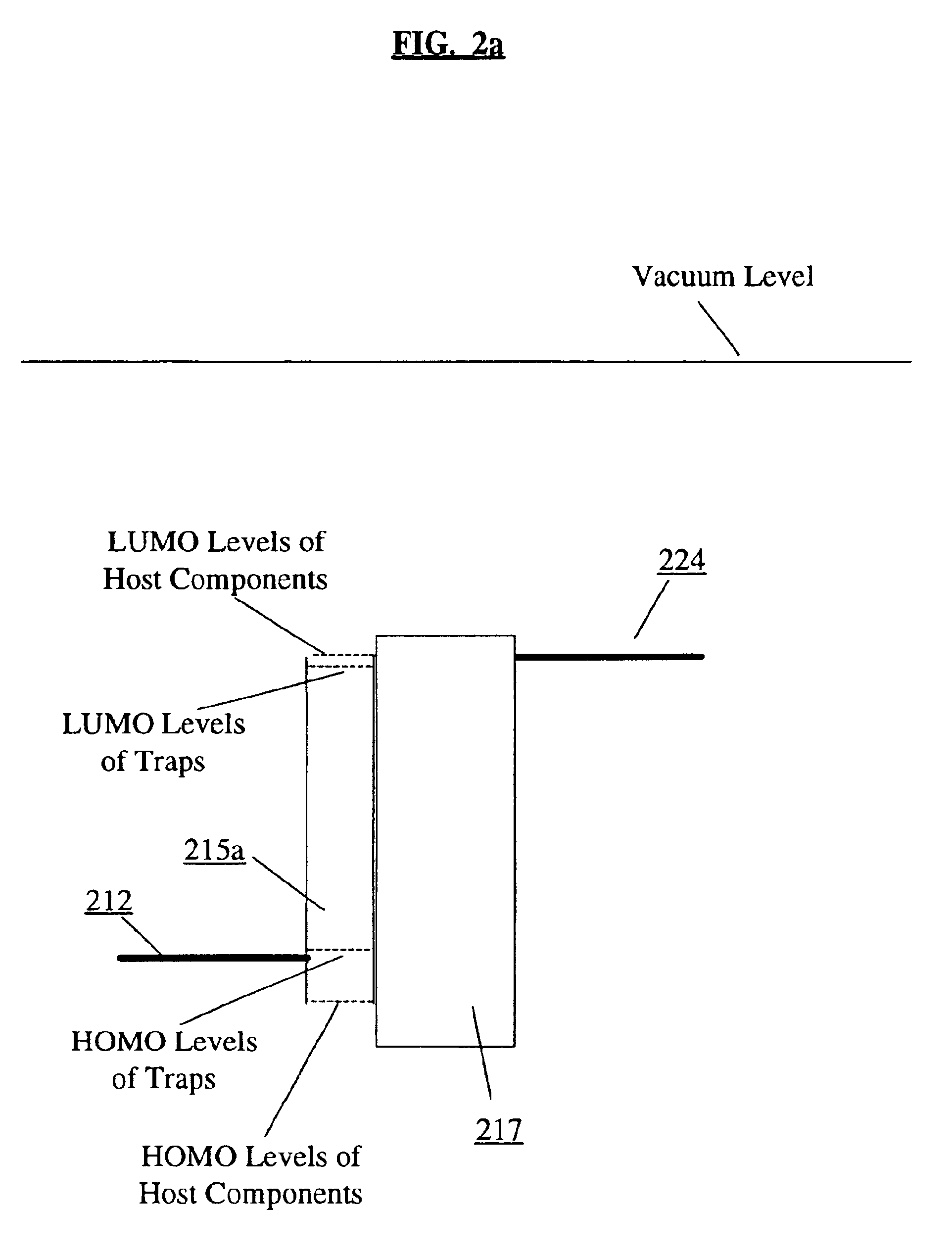
[0011]In an embodiment of the invention, an electronic device includes an interfacial layer with traps. This interfacial layer is between an electrode and an organic layer, and if the electrode was adjacent to the organic layer, the energy barrier between these two layers is such that the current through the organic layer is limited by charge injection into this layer rather than the transport properties of the organic layer. The traps are used to accumulate charges of one charge type (e.g., either electrons or holes) within the interfacial layer. By accumulating charges, the bands of the interfacial layer are bent so that charges can tunnel from the electrode to the organic layer thus increasing the efficiency of the electronic device and allowing organic layers to be used within an electronic device that otherwise would be too inefficient for use in that device.

[0012]FIG. 1 shows a cross-sectional view of an embodiment of an electronic device 205 according to the present invention...


PUM

PropertyMeasurementUnit
work functionaaaaaaaaaa
thicknessaaaaaaaaaa
thicknessaaaaaaaaaa

Abstract

In an embodiment of the invention, an electronic device includes an interfacial layer with traps. This interfacial layer is between an electrode and an organic layer, and if the electrode was adjacent to the organic layer, the energy barrier between these two layers is such that the current through the organic layer is limited by charge injection into this layer rather than the transport properties of the organic layer. The traps are used to accumulate charges of one charge type (e.g., either electrons or holes) within the interfacial layer. By accumulating charges, the bands of the interfacial layer are bent so that charges can tunnel from the electrode to the organic layer thus increasing the efficiency of the electronic device and allowing organic layers to be used within an electronic device that otherwise would be too inefficient for use in that device.

Description

BACKGROUND OF THE INVENTION[0001]An organic light emitting diode (“OLED”) display can include, for example, the following: (1) an anode on a substrate; (2) an emissive layer on the anode; and (3) a cathode on the emissive layer. When the display is forward biased, holes are injected from the anode into the emissive layer, and the electrons are injected from the cathode into the emissive layer. Both carriers recombine with each other, the location of which is called the recombination zone; the recombinations in the emissive layer produce visible light. The power efficiency of the device is controlled by many factors, two of which are (1) the radiative recombination efficiency, and (2) the operating voltage. Radiative recombination efficiency is the ratio of the number of electrons and holes that result in the emission of a photon per unit time to the ratio of the total current (number of holes and electrons flowing through the film per unit time). In order to inject the electrons and...

Claims


Application Information

Patent Timeline
Patent Type & Authority Patents(United States)
IPC IPC(8): H01L29/24H01L29/167H01L35/12H01L29/207H01L29/02H01L31/062H01L31/06H01L35/24H01L51/00H01L51/50
CPCH01L51/5088H01L51/5092H01L51/0034H01L51/0035H01L51/0036H01L51/0039H01L51/0043H10K85/10H10K85/115H10K85/111H10K85/151H10K85/113H10K50/171H10K50/17
Inventor GUPTA, RAHULPSCHENITZKA, FLORIANCHOONG, VI-ENALLEMAND, PIERRE-MARC
Owner DOLYA HOLDCO 5 LTD
Why Eureka
Try Eureka