

Semiconductor package for memory chips
- Summary
- Abstract
- Description
- Claims
- Application Information
AI Technical Summary
Benefits of technology
Problems solved by technology
Method used
Image

Examples
first embodiment
[0025]FIGS. 2A to 2D show the fabrication processes for the MMC package in accordance with the present invention.
[0026]Referring to FIG. 2A, the first step is to prepare a substrate strip 100 comprising an array of integrally formed substrates 110. Each of the substrates 110 includes at least one chip attach area 111, a plurality of passive component attach areas 112 (optional), and a plurality of electrical connection pads 113. The electrical connection pads 113 each extends from a top surface to a bottom surface of the substrate 110 to serve as contacts for external electrical connection for the MMC package.
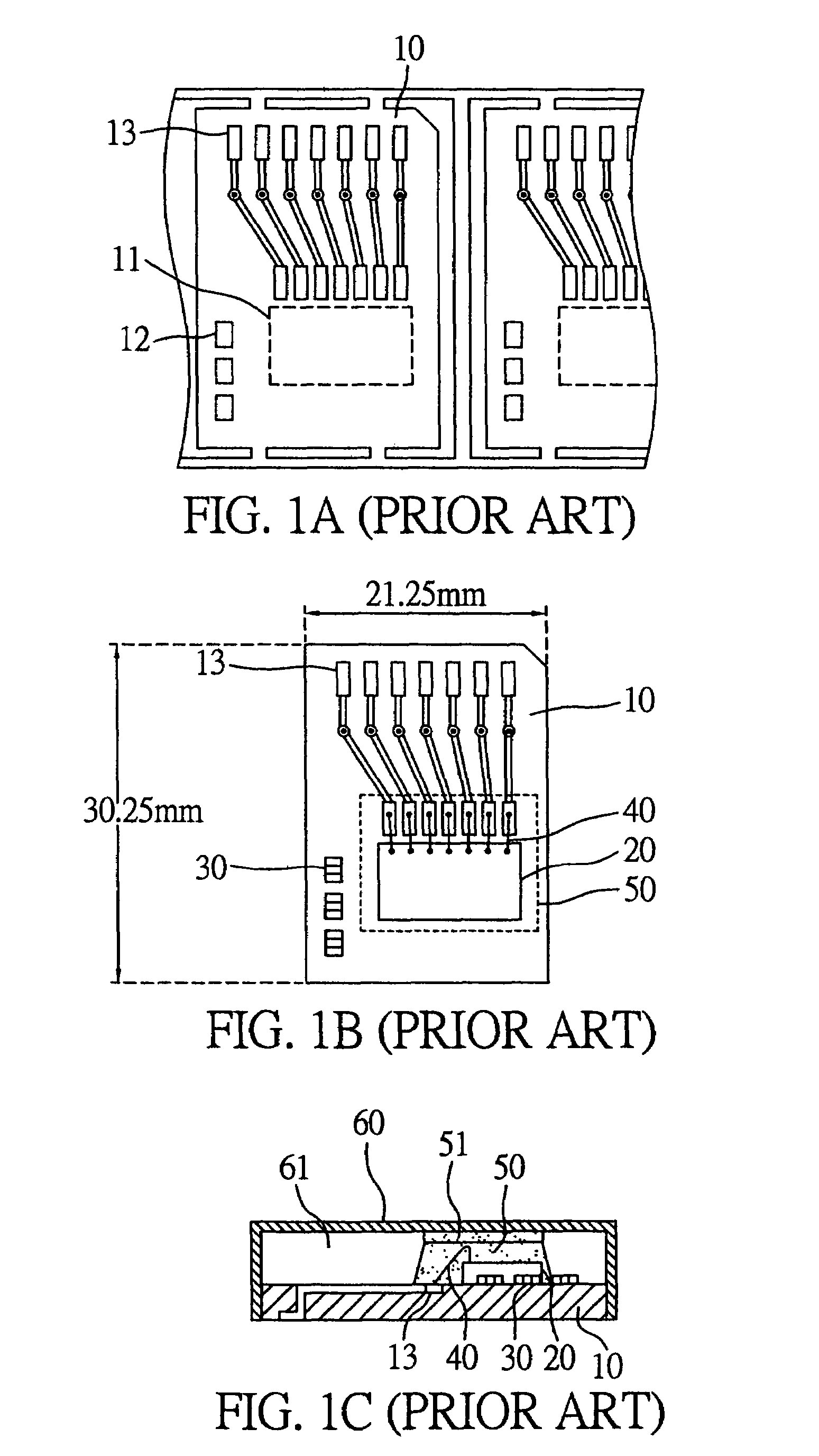
[0027]The substrate strip 100 is substantially sized 56 mm (length)×56 mm (width), and is pre-defined into 15 substrates 110 (5×3), each of the substrates 110 substantially having dimensions of 18 mm (length)×10 mm (width).
[0028]Referring to FIG. 2B, a die-bonding process is performed to mount two stacked chips 120 on the chip attach area 111 of each of the substrates 110 (only...
second embodiment
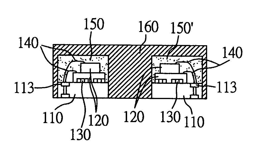
[0033]The MMC package of the second embodiment comprises two substrates 110, each having a chip attach area and a plurality of electrical connection pads 113; at least two stacked chips 120 mounted on the chip attach area of each of substrates 110 and electrically connected to the electrical connection pads 113; an encapsulation body 150 formed on each of the substrates 110 for encapsulating the chips 120; and a rectangular cover 160 for receiving the two substrates 110, chips 120 and encapsulation bodies 150 therein. The longer side of each of the substrates 110 is vertical to the longer side of the cover 160. The electrical connection pads 113 on the two substrates 110 are exposed on the opposite surfaces (top and bottom surfaces) of the cover 160. This allows the fabricated MMC package to have two opposite plug terminals for dual usage and have doubled memory capacity.
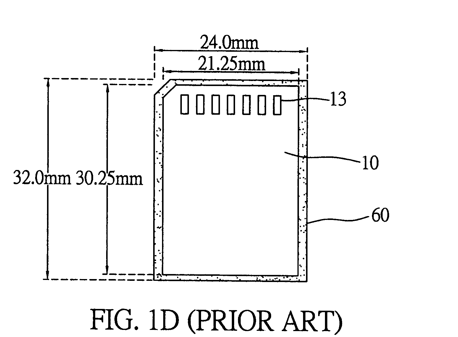
[0034]As compared to the prior art, the MMC package according to the present invention uses smaller substrates si...
PUM
 Abstract
Description
Claims
Application Information