Method of driving plasma display panel by applying discharge sustaining pulses

a plasma display panel and plasma technology, applied in the direction of gas discharge vessels/containers, instruments, static indicating devices, etc., can solve the problem of limited degree to which the pixel pitch can be reduced, the scale of the drive circuit must be large, and the stumbling block to achieve high definition. achieve the effect of increasing the number of gradations and increasing the brightness

Inactive Publication Date: 2005-11-15
HITACHI PLASMA PATENT LICENSING
View PDF27 Cites 10 Cited by
  • Summary
  • Abstract
  • Description
  • Claims
  • Application Information

AI Technical Summary

Benefits of technology

[0015]Accordingly, a comprehensive object of the present invention is to provide a plasma display panel, a method of driving same and a plasma display apparatus, which achieve a higher quality image.
[0016]To put it concretely, a first object of the present invention is to provide a method of driving a plasma display panel and a plasma display apparatus, which achieve higher definition by further reducing a pixel pitch.
[0017]A second object of the present invention is to provide a plasma display panel, a method of driving the same and a plasma display apparatus that can increase black display quality reduced by whole-screen (all pixel) discharge light emission during a reset period.

Problems solved by technology

However, since a pair of electrodes is provided for each of the display lines L1 to L5, the degree to which the pixel pitch can be reduced is limited and this is a stumbling block for achieving high definition.
In addition, the scale of the drive circuit must be large since there is a high number of electrodes.
However, in the publications cited above, since write is performed in linear sequence for the display lines L1 to L8, the discharge would affect adjacent pixels in the direction of the address electrodes if the partitioning walls 191 to 199 are omitted, resulting in erroneous display.
Thus, the partitioning walls 191 to 199 cannot be omitted and this presents an obstacle to achieving higher definition by reducing the pixel pitch.
In addition, it is not easy to provide the partitioning walls 191 to 199 on the central lines of the electrodes and, as a result, the PDP 10Q will be expensive to produce.
Furthermore, in the publications mentioned above, a specific waveform of the voltage to be applied to the electrodes is not disclosed and, as a result, the invention has not been put into practical use.
In addition, during the reset period, light is emitted because of the whole-screen (all pixel) discharge and brightness in the black display areas is increased, reducing the quality of the display.
Moreover, since the color of the phosphor is white or bright gray, incident light from the outside is reflected on the phosphor at non display line when observing an image on the PDP in bright place, lowering the contrast of the image.
In addition, since only one line can be addressed at a time, the address time cannot be reduced, and it is not possible to achieve a higher number of gradations by increasing the number of subfields or to achieve higher brightness by increasing the number of times sustaining discharge is performed.

Method used


Image

  • Method of driving plasma display panel by applying discharge sustaining pulses
  • Method of driving plasma display panel by applying discharge sustaining pulses
  • Method of driving plasma display panel by applying discharge sustaining pulses

Examples


first embodiment

[0083

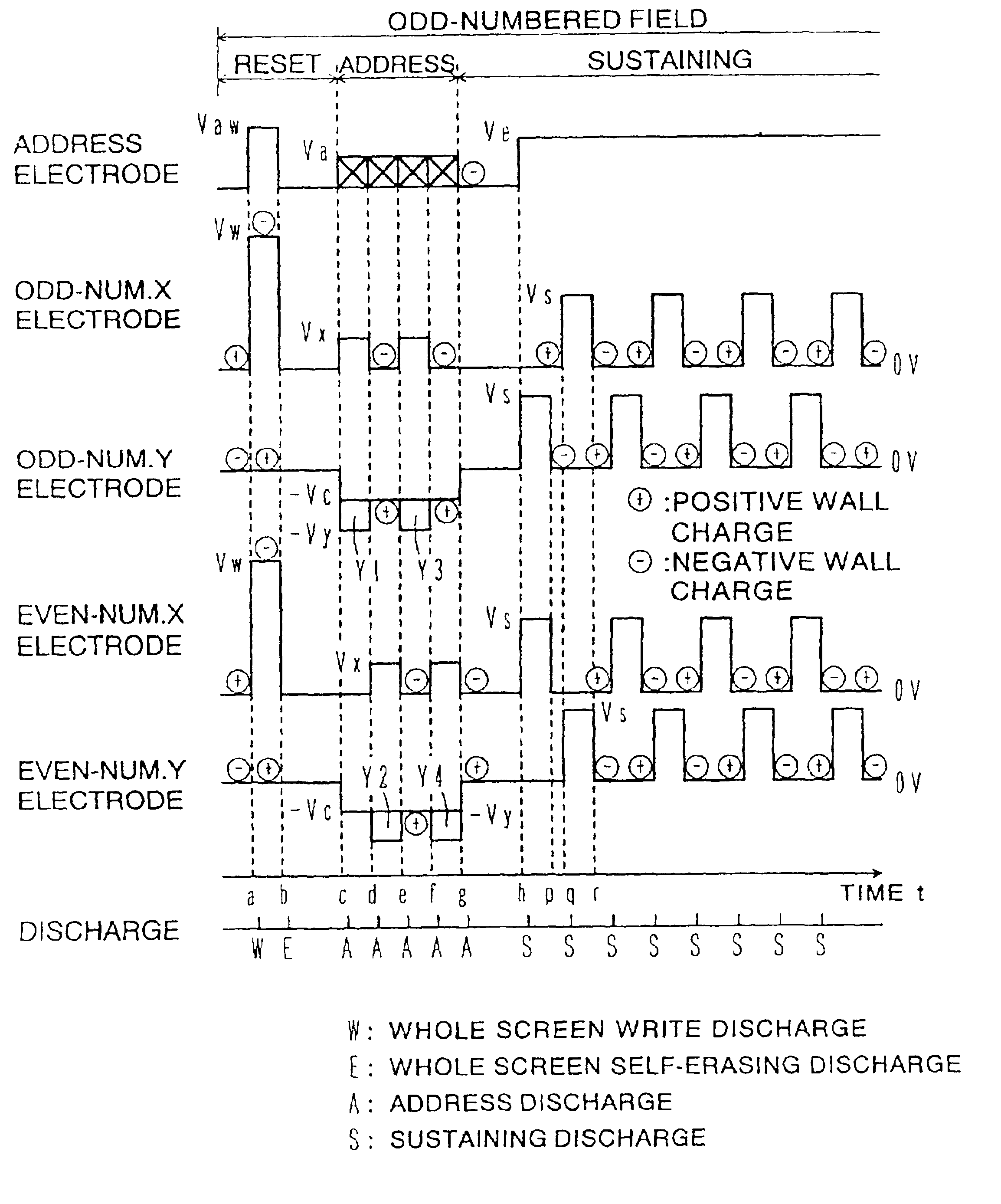
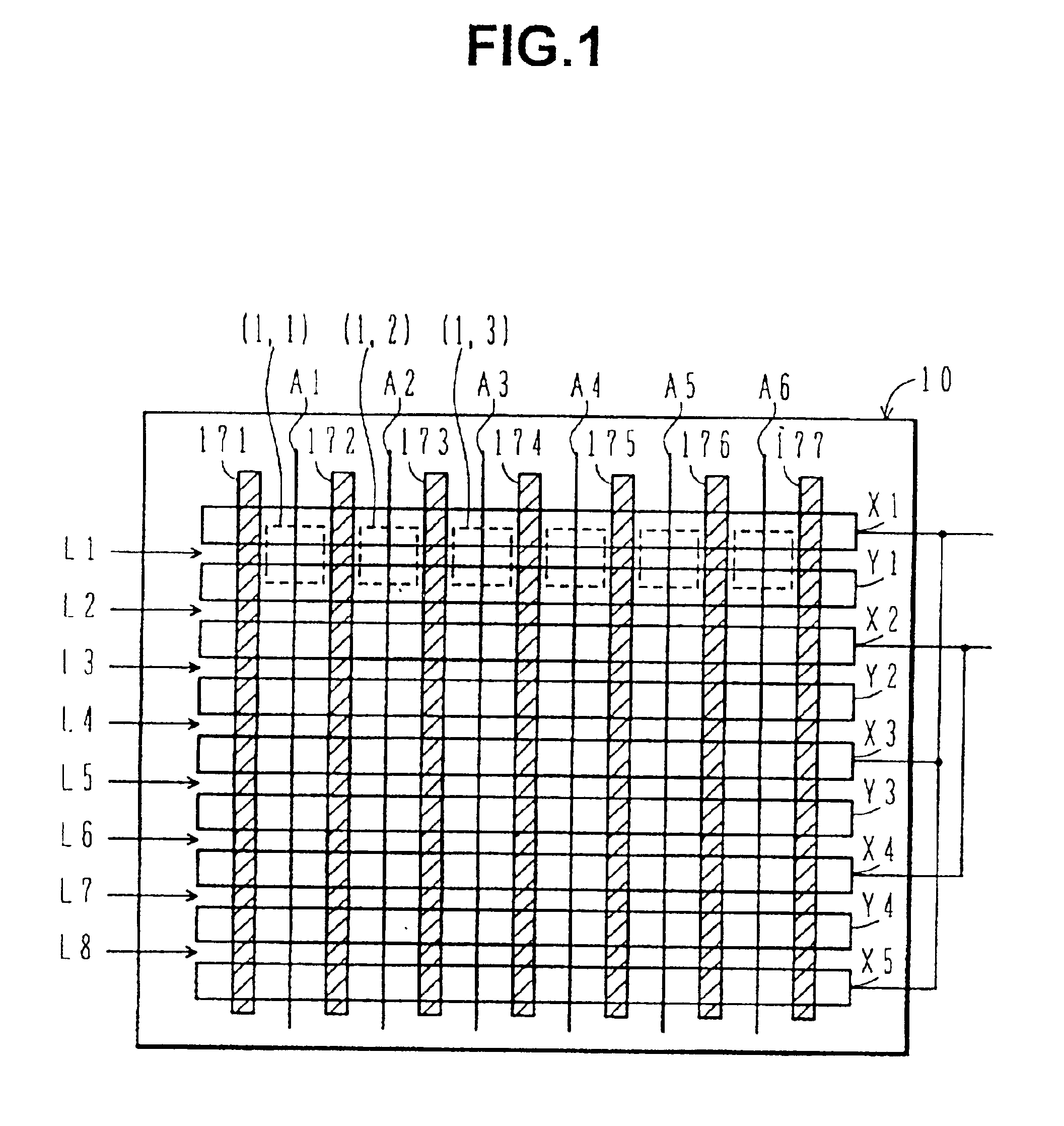
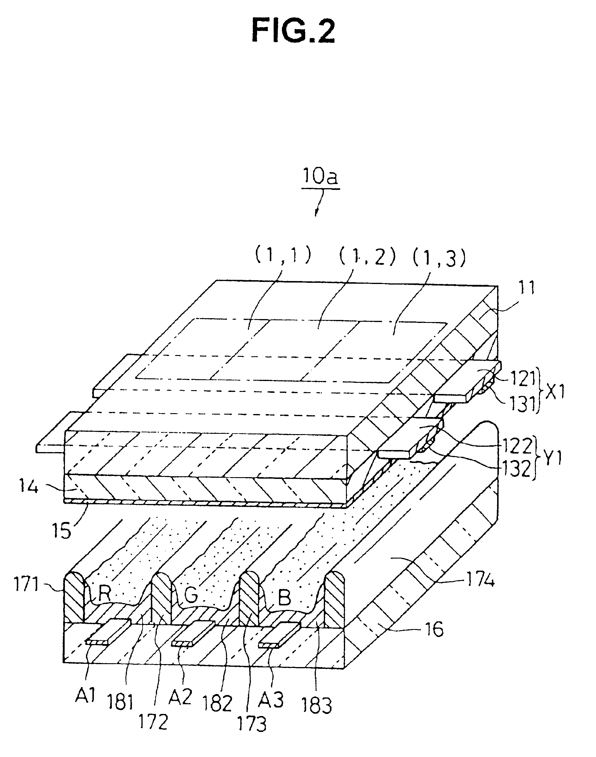
[0084]FIG. 1 shows a PDP 10 in the first embodiment according to the present invention. In FIG. 1, pixels are indicated with dotted lines only for display line L1. In order to simplify the explanation, the number of pixels of the PDP 10 is 6×8=48 monochromatic pixels. The present invention may be applied to both color and monochromatic pixels and three monochromatic pixels corresponds to one color pixel.

[0085]In order to facilitate production and to achieve higher definition by reducing the pixel pitch, the PDP 10 has a structure in which the partitioning walls 191 to 199 in the PDP 10Q in FIG. 31 are removed. In order to ensure that erroneous discharge does not occur among adjacent display lines due to the removal of the partitioning walls, interlaced scanning is performed in such a manner that the phases of the waveforms of the sustaining pulse voltages in the odd-numbered lines and in the even-numbered lines among the electrodes L1 to L8, which perform surface discharge and ...

second embodiment

[0133

[0134]If the number of pulses can be reduced in FIGS. 7 and 8, power consumption can also be reduced. During an address period, if the pulses supplied to the odd-numbered X electrodes and the even-numbered X electrodes are made to be continuous, the number of pulses can be reduced. This can be achieved by performing scanning in the order shown in FIG. 6(B). To be more specific, the display lines L1, L3, L5 and L7 in the odd-numbered field should be further divided into odd-numbered lines and even-numbered lines and after scanning one group sequentially, the other group should be scanned sequentially. The same procedure is performed for the even-numbered field.

[0135]FIG. 9 shows the schematic structure of a plasma display apparatus 20A in the second embodiment for implementing this method.

[0136]During an address period, in order to perform scanning in the order of the electrodes Y1, Y3, Y2 and Y4, the output of the driver 232(2) is connected to the electrode Y3 and the output of...

third embodiment

[0139

[0140]In FIG. 7, the common pulse at the voltage Vx is supplied to the electrodes X1, X3 and X5 and the common pulse at the voltage Vx is supplied to the electrodes X2 and X4. However, it suffices to supply a pulse at the voltage Vx to the electrodes X1 to X4 selected sequentially when the electrodes Y1 to Y4 are selected sequentially. In this way, the number of pulses supplied to the electrodes is reduced and power consumption is also reduced.

[0141]To achieve the above in a plasma display apparatus 20B in the third embodiment, a scanning circuit 30 is provided for the X electrodes, too, as shown in FIG. 12. The scanning circuit 30 is different from the scanning circuit 23 only in that the number of components is larger by the equivalent of one electrode.

[0142]During an address period, “1” is provided to the data input for bit 301(1) in the odd-numbered field and “1” is provided to the data input for bit 301(2) in the even-numbered field at a shift register 301 from a control c...


PUM


Abstract

Method for driving a plasma display panel. At least one first discharge sustaining pulse is applied to a first pair of display electrodes, and at least one second discharge sustaining pulse applied to an adjacent pair of display electrodes. The first and second discharge sustaining pulses are applied such that they are in the same phase as one another and / or such that a current in the first pair of display electrodes flows in the opposite direction from a current in the adjacent pair of display electrodes.

Description

[0001]This Application is a divisional of application Ser. No. 08 / 690,038, filed Jul. 31, 1996, now U.S. Pat. No. 6,373,452, issued Apr. 16, 2002.BACKGROUND OF THE INVENTION[0002]1. Field of the Invention[0003]The present invention relates to a surface discharge AC plasma display panel, a method of driving same and a plasma display apparatus employing same.[0004]2. Description of the Related Art[0005]The plasma display panel (PDP) has good visibility because it generates its own light, is thin and can be made with large-screen and high-speed display. For these reasons it is attracting interest as a replacement for the CRT display. A surface discharge AC PDP is especially suitable for full color display. Therefore, there are high expectations in the field of high-vision and the demand for a higher quality image is increasing. A higher quality image is achieved by generating higher definition, a higher number of gradations, better brightness, lower brightness for black areas, higher c...

Claims


Application Information

Patent Timeline
Patent Type & Authority Patents(United States)
IPC IPC(8): G09G3/28H01J17/49G09G3/20G09G3/292G09G3/293G09G3/294G09G3/296G09G3/298G09G3/299
CPCG09G3/2932G09G3/294G09G3/2948G09G3/296G09G3/2983G09G3/299H01J11/12H01J11/28H01J11/44G09G3/2018G09G3/292G09G3/293G09G2310/0205G09G2310/0218G09G2310/0221G09G2310/0224G09G2330/021H01J2211/444G09G2230/00
Inventor ISHII, TOMOYUKIHIROSE, TADATSUGUKANAZAWA, YOSHIKAZUUEDA, TOSHIOKISHI, TOMOKATSUTOMIO, SHIGETOSHIASAMI, FUMITAKA
Owner HITACHI PLASMA PATENT LICENSING
Why Eureka
Try Eureka