

Non-volatile static random access memory
a random access memory and non-volatile technology, applied in static storage, digital storage, instruments, etc., can solve the problems of non-volatile semiconductor memory being slower to operate than volatile memory, sram is typically more expensive to manufacture than dram, loss of data, etc., and achieve the effect of improving memory device and method
- Summary
- Abstract
- Description
- Claims
- Application Information
AI Technical Summary
Benefits of technology
Problems solved by technology
Method used
Image

Examples
embodiment 200
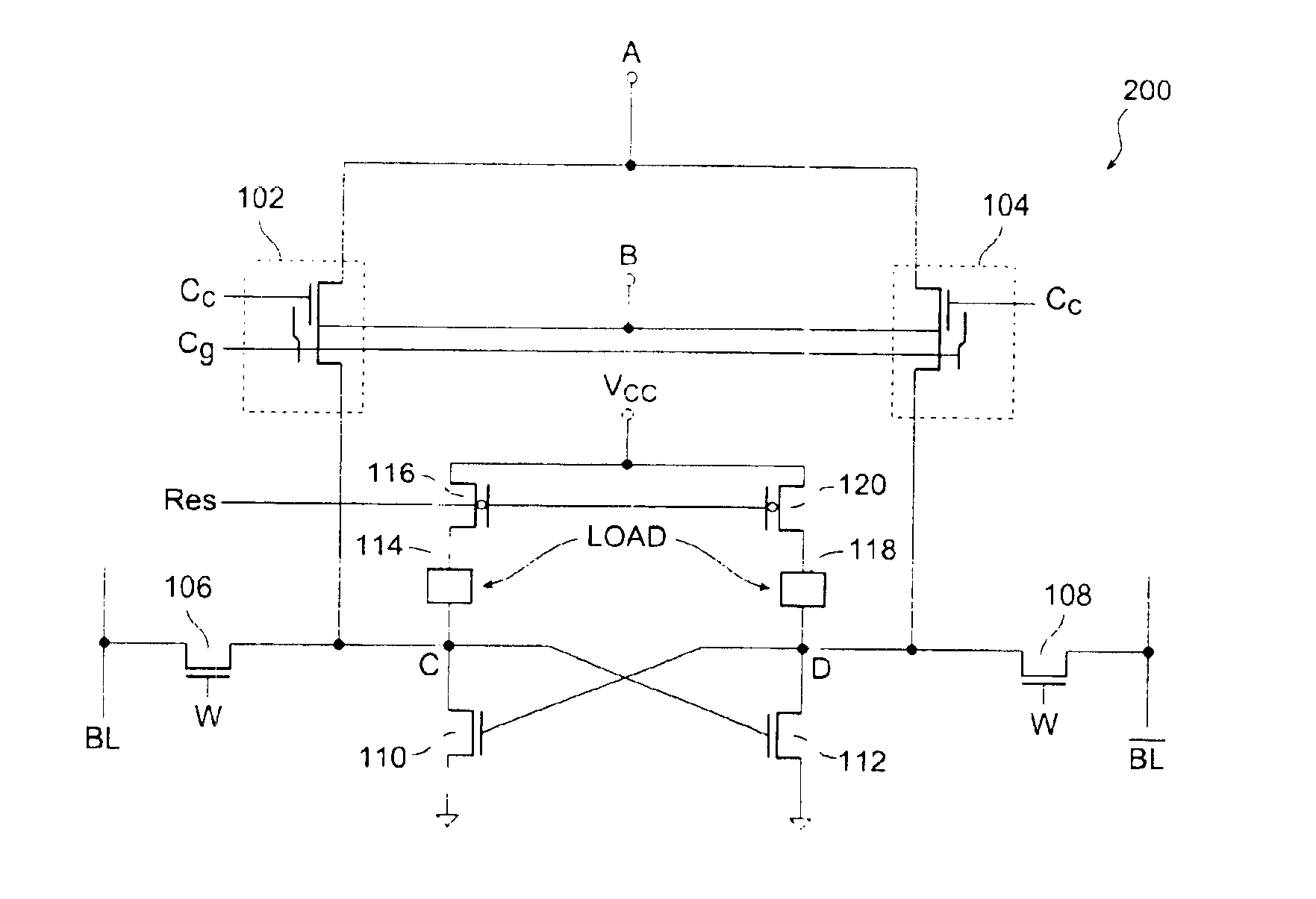
[0063]FIG. 8 shows a schematic diagram of a non-volatile SRAM 200, in accordance with another embodiment of the present invention. Non-volatile SRAM 200 is similar to non-volatile SRAM 100 except that includes resistive loads 114, 118 and transistors 116, 120. Resistive load 114 has a first terminal coupled to node C and a second terminal coupled to the drain (source) terminal of MOS transistor 116. The source (drain) terminal of MOS transistor 116 is supplied to the supply voltage Vcc. Resistive load 118 has a first terminal coupled to node D and a second terminal coupled to the drain (source) terminal of MOS transistor 120. The source (drain) terminal of MOS transistor 120 is supplied to the supply voltage Vcc. Signal RES is applied to the gate terminals of MOS transistors 116, 120. In the embodiment 200, MOS transistors 116 and 120 are shown as being PMOS transistors. It is understood, however, that MOS transistors 116, 120 may be NMOS transistors. In the description below, it is...
embodiment 300
[0065]FIG. 9 shows a schematic diagram of a non-volatile SRAM300, in accordance with another embodiment of the present invention. Non-volatile SRAM 300 is similar to non-volatile SRAM 100 except that includes PMOS transistors 114, 116, 118. PMOS transistor 114 has a source terminal coupled to the drain terminal of PMOS transistor 118, a drain terminal coupled to the drain terminal of NMOS transistor 110, and a gate terminal coupled to the gate terminal of NMOS transistor 110. PMOS transistor 116 has a source terminal coupled to the drain terminal of PMOS transistor 118, a drain terminal coupled to the drain terminal of NMOS transistor 112, and a gate terminal coupled to the gate terminal of NMOS transistor 112. The source terminal of PMOS transistor 118 is supplied to the supply voltage Vcc. Signal RES is applied to the gate terminals of PMOS transistor 118. In the embodiment 300, MOS transistors 114, 116 and 118 are shown as being PMOS transistors. It is understood, however, that M...
PUM
 Abstract
Description
Claims
Application Information