Device transfer mechanism for a test handler

a technology of transfer mechanism and test handler, which is applied in the direction of individual semiconductor device testing, transportation and packaging, instruments, etc., can solve the problems of increasing the risk of failure, increasing the complexity of the task of handling them properly and efficiently, and requiring too many rotation arms, so as to reduce the number of transfer components and reduce the effect of area

Active Publication Date: 2005-11-22
ASM ASSEMBLY AUTOMATION LTD
View PDF6 Cites 30 Cited by
  • Summary
  • Abstract
  • Description
  • Claims
  • Application Information

AI Technical Summary

Benefits of technology

[0006]The invention seeks to provide an improved transfer mechanism with a simpler structure by reducing the number of transfer components. Thus, it also seeks to occupy a smaller area as compared to the prior art while providing greater alignment precision.

Problems solved by technology

As these packages are getting ever-smaller in size, the task of handling them properly and efficiently becomes more difficult and complex.
This design requires too many rotation arms.
With more components comprised in the transfer mechanism, there is a correspondingly increased risk of failure.

Method used


Image

  • Device transfer mechanism for a test handler
  • Device transfer mechanism for a test handler
  • Device transfer mechanism for a test handler

Examples


Embodiment Construction

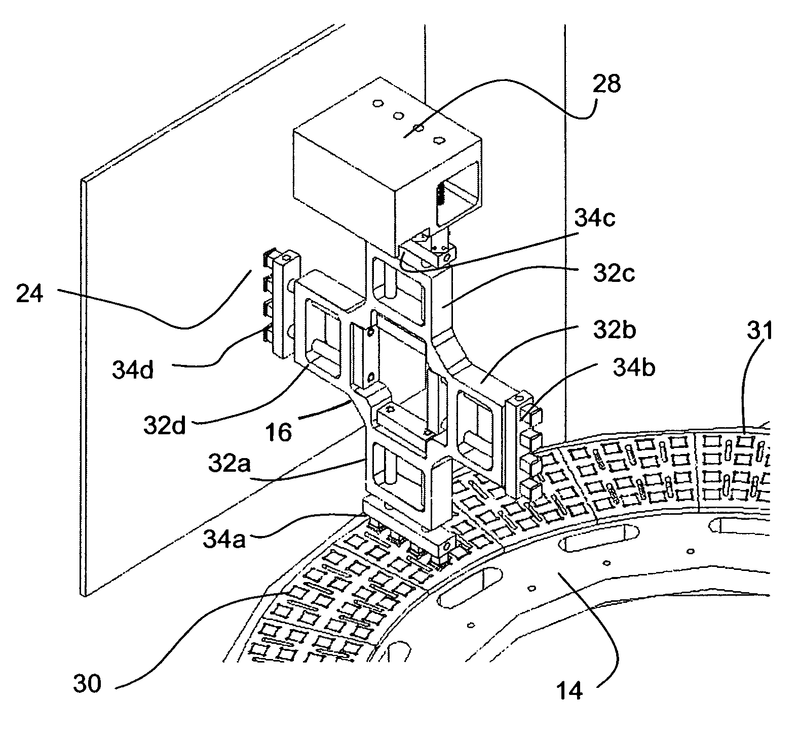
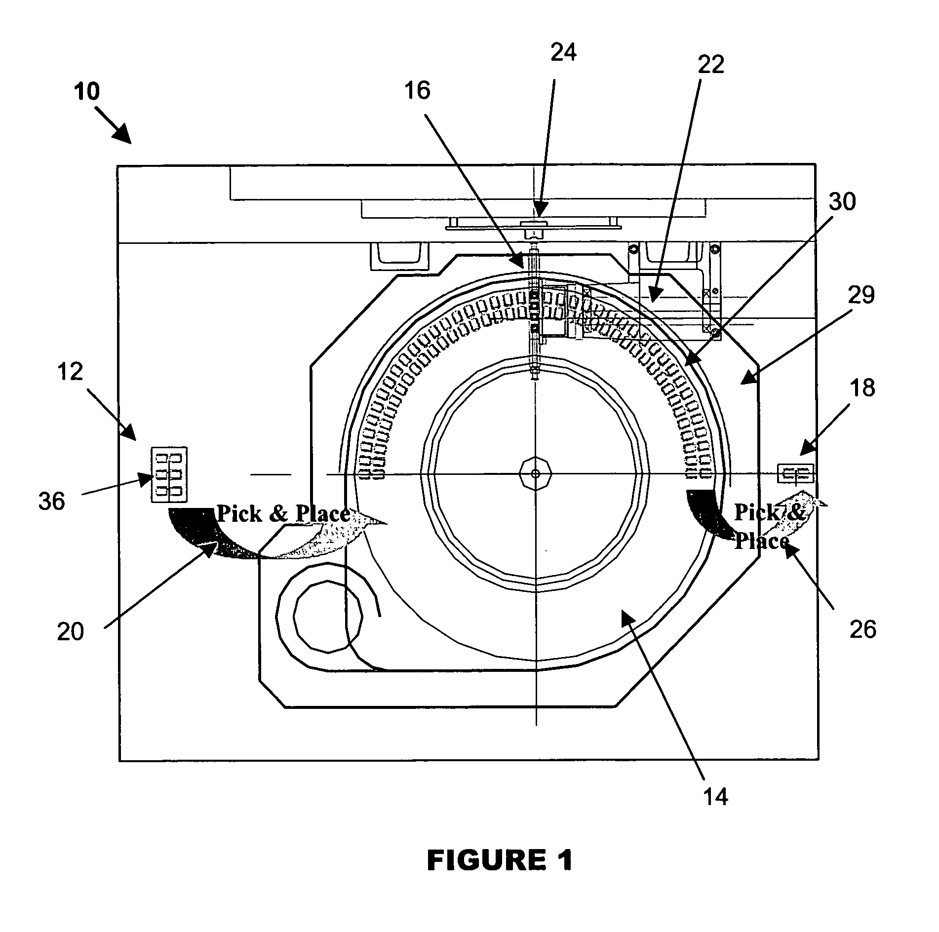
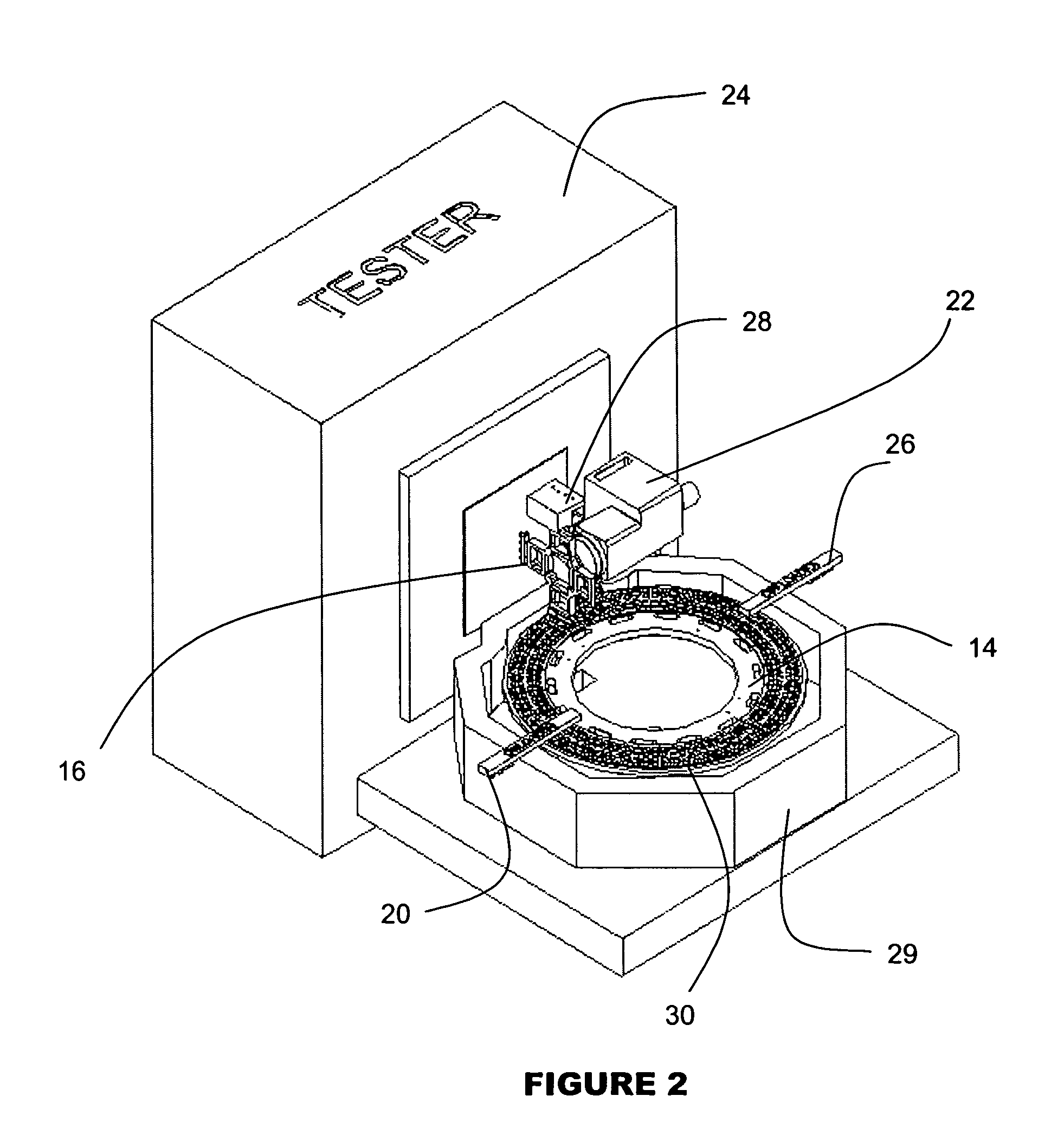
[0016]FIG. 1 is a plan view of a test handler 10 illustrating the layout of a device transfer mechanism according to the preferred embodiment of the invention. The test handler 10 includes an input buffer 12 at an input location, a thermally-enclosed section surrounded by a thermal insulation wall 29, a platform in the form of a round turntable 14, a transfer arm in the form of a rotary transfer arm 16 and an output buffer 18 at an output location.

[0017]Semiconductor or IC devices 36 are placed into the input buffer 12 from an upstream process. The input buffer 12 consists of several columns of pockets for holding and staging the devices 36. The devices 36 are moved by an onloading transfer arm 20 to an onloading position on the turntable 14. The onloading transfer arm 20 comprises a number of suction pick heads. In a typical cycle, the onloading transfer arm 20 moves over the input buffer 12, positions its pick heads directly above the devices 36, moves down and picks up the device...


PUM


Abstract

The invention provides a mechanism for a test handler using for electrical testing of electronic devices. The devices are placed on a platform configured to move semiconductor devices from an onloading position to an offloading position along a predetermined path. A transfer arm with a plurality of transfer heads connected to it is located adjacent the path. The transfer heads are configured to pick up and transfer semiconductor devices from the platform to a testing position for testing, and thereafter to transfer the semiconductor devices from the testing position to the platform for offloading.

Description

FIELD OF THE INVENTION[0001]The invention relates to a mechanism for moving devices, in particular semiconductor or integrated circuit (“IC”) devices, between different locations in a test handler used for testing the devices.BACKGROUND AND PRIOR ART[0002]In the automated assembly and packaging of semiconductor or IC devices, the function of a test handler is to test the packaged devices, preferably after they are separated both electrically and physically from one another. There are many types of IC packages in the art, such as chip-scale packages. Commonly, the packaged devices are tested in bulk in order to increase throughput and thus a plurality of these packages need to be handled together simultaneously. As these packages are getting ever-smaller in size, the task of handling them properly and efficiently becomes more difficult and complex.[0003]Typically, the packages are transferred from an input position, moved near to a tester, precisely positioned and aligned with respec...

Claims


Application Information

Patent Timeline
Patent Type & Authority Patents(United States)
IPC IPC(8): G01R1/00G01R31/26G01R31/28
CPCG01R31/2893
Inventor TSUI, CHING MAN STANLEYSZE, CHAK TONG ALBERTTSAI, PEI WEICHOW, LAP KEI ERIC
Owner ASM ASSEMBLY AUTOMATION LTD
Why Eureka
Try Eureka