High yield reticle with proximity effect halos

Inactive Publication Date: 2005-11-22
SYNOPSYS INC
View PDF35 Cites 217 Cited by
  • Summary
  • Abstract
  • Description
  • Claims
  • Application Information

AI Technical Summary

Benefits of technology

[0021]In one embodiment, the proximity effect halo includes an inner perimeter and an outer perimeter, wherein a distance between the inner perimeter and the outer perimeter is substantially constant. The lithographic process in which the reticle will be used can determine this distance. Specifically, a reticle is generally used in a lithography process using an exposing radiation of a substantially constant wavelength and having a substantially constant numerical aperture (NA). In this case, the distance can be estimated by dividing the wavelength by the NA and multiplying the result by a constant correction factor to compensate for resist and etch effects. For example, the distance is approximately equal to 1.5 microns when the substantially constant wavelength is 365 nm and the NA is 0.6. In another example, the distance is approximately equal to 1.0 microns when the substantially constant wavelength is 248 nm and the NA is 0.6. In yet another example, the distance is between 3.0 μm and 3.75 μm for a 50 keV electron beam reticle writing process.
[0022]According

Problems solved by technology

Also, the dimensions and regularity of a printed image can be affected by portions of adjacent features or even by nearby defects.
Resist and etch effects can further add to the proximity effects, though such pr

Method used


Image

  • High yield reticle with proximity effect halos
  • High yield reticle with proximity effect halos
  • High yield reticle with proximity effect halos

Examples


Example

DETAILED DESCRIPTION OF THE DRAWINGS

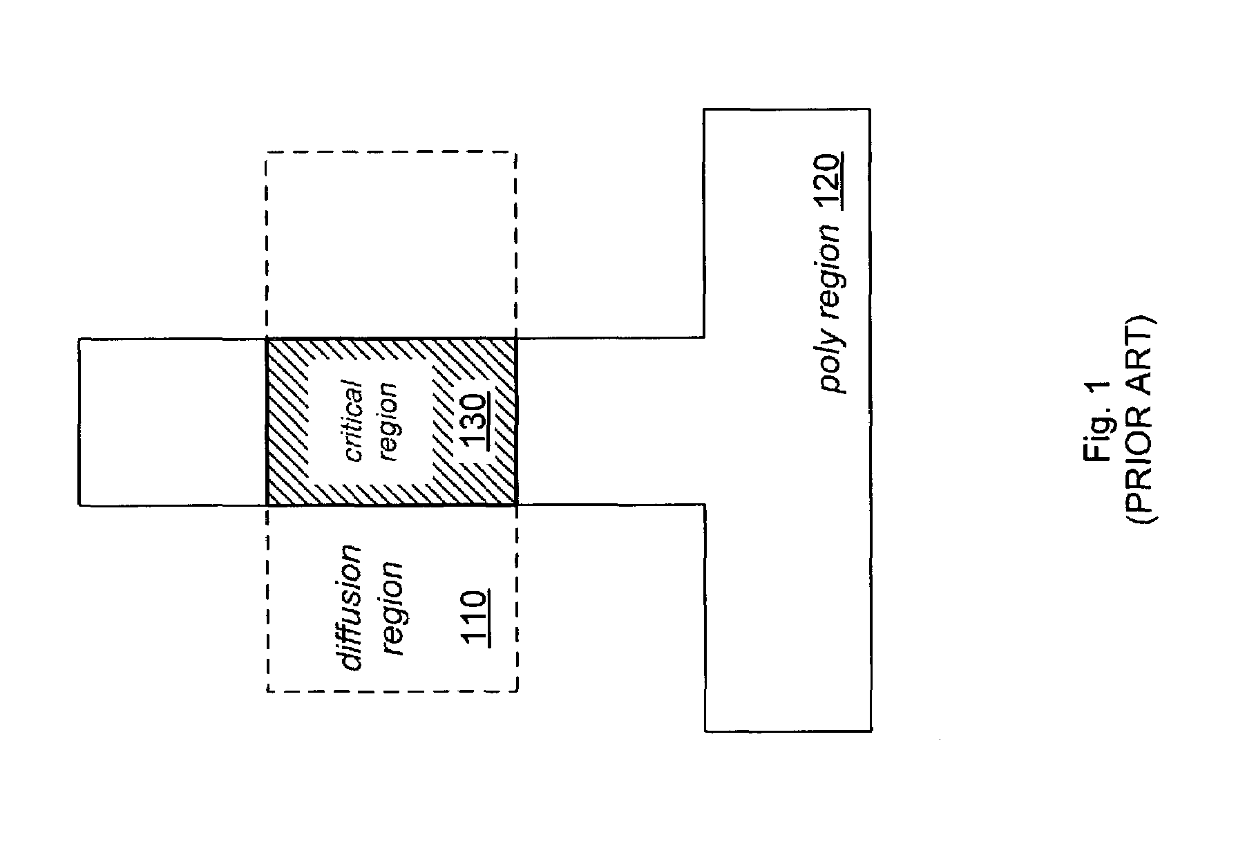
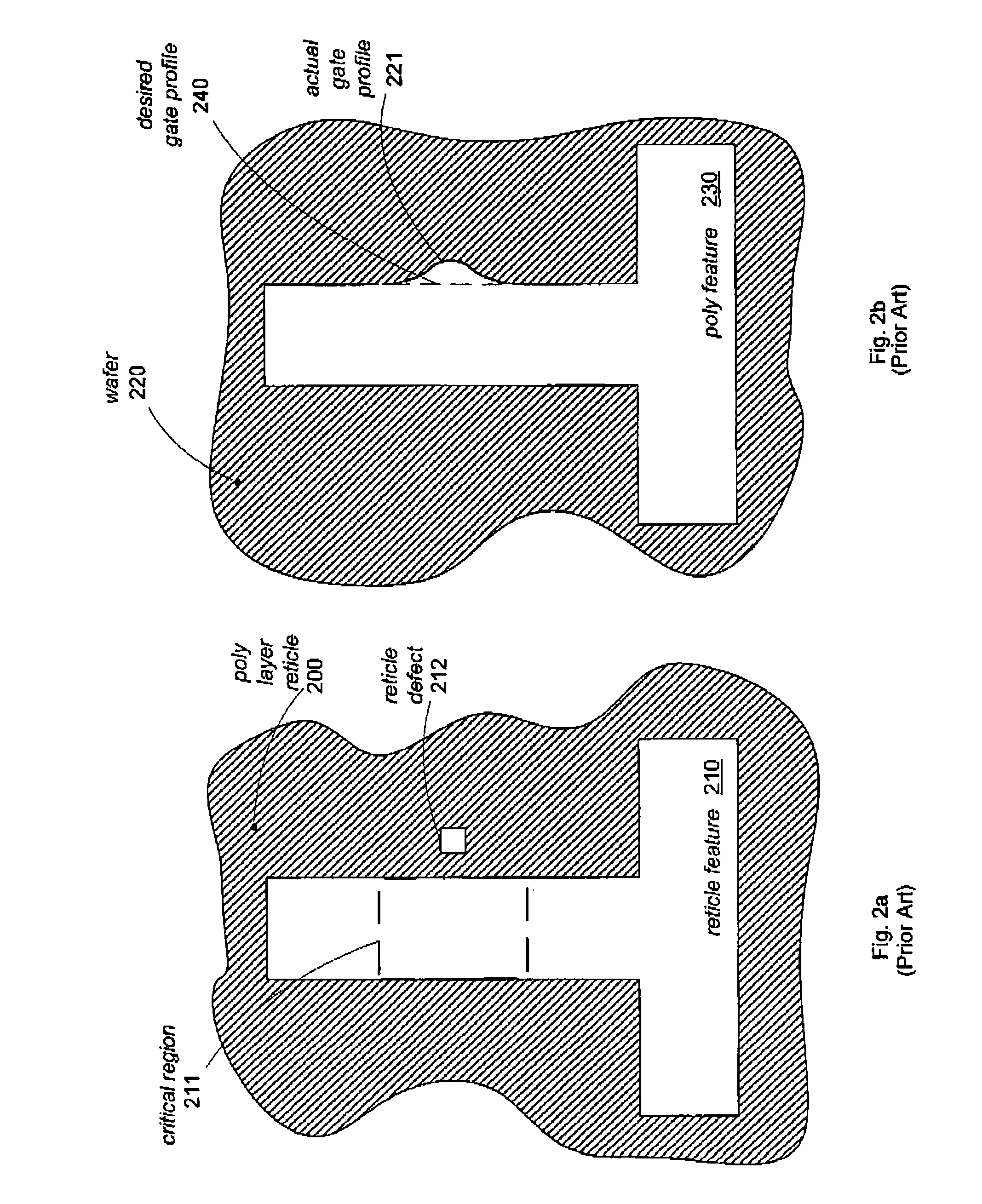
[0031]FIG. 3 provides an example of a “tight tolerance feature” that could require special attention during reticle writing to ensure proper device formation during lithography. FIG. 3 shows sample layout features 310 and 320 that can commonly be found in a conventional IC layout design. As depicted in FIG. 3, layout feature 320 represents a feature to be formed in a polysilicon layer of an IC, over a diffusion region represented by layout feature 310. Layout features 310 and 320 therefore designate a transistor to be formed in the IC, the gate of the transistor being defined where layout feature 320 overlies layout feature 310. Accordingly, layout feature 320 includes a tight tolerance feature 321 that corresponds to this overlap region. Tight tolerance feature 321 must be accurately formed in the final IC since the gate of a transistor is so critical to device performance.

Proximity Effect Halo

[0032]To ensure this accurate formation of tight tole...


PUM


Abstract

A lithography reticle advantageously includes “proximity effect halos” around tight tolerance features. During reticle formation, the tight tolerance features and associated halos can be carefully written and inspected to ensure accuracy while the other portions of the reticle can be written/inspected less stringently for efficiency. A system for creating a reticle data file from an IC layout data file can include a processing module and a graphical display. The processing module can read the IC layout data file, identify critical features and define a halo region around each of the critical features. The graphical user interface can facilitate user input and control. The system can be coupled to a remote IC layout database through a LAN or a WAN.

Description

RELATED APPLICATIONS[0001]This application is a divisional of U.S. patent application Ser. No. 09 / 676,400, now U.S. Pat. No. 6,557,162, entitled, “Method For High Yield Reticle Formation”, filed on Sep. 29, 2000 incorporated by reference herein.FIELD OF THE INVENTION[0002]The present invention relates to semiconductor device manufacturing and specifically to the efficient production of reticles for lithographic processes.BACKGROUND OF THE INVENTION[0003]Lithography masks (or “reticles”) are key elements used in the production of integrated circuits (ICs). A portion of an IC layout data file (typically a representation of a physical layer, such as a metal layer or a polysilicon layer, of the final IC) is etched into a thin chrome layer formed over a glass plate to form a reticle. This reticle pattern (“reticle layout”) is then exposed onto a layer of photosensitive resist on the surface of the wafer. Finally, the top surface of the wafer is chemically etched away in the areas not cov...

Claims


Application Information

Patent Timeline
IPC IPC(8): G03F1/62G03F1/68G03F7/20H01J37/302H01L21/027
CPCG03F1/144G03F7/2059H01J37/3023H01J2237/31769G03F1/36G03F1/62G03F1/68
Inventor PIERRAT, CHRISTOPHE
Owner SYNOPSYS INC
Why Eureka
Try Eureka