Semiconductor device and method for manufacturing the same

Inactive Publication Date: 2005-11-29
INVENSAS CORP
View PDF3 Cites 12 Cited by
  • Summary
  • Abstract
  • Description
  • Claims
  • Application Information

AI Technical Summary

Benefits of technology

[0005]The present invention is achieved in consideration of such points and an object thereof is to provide a semiconductor device and a method for manufacturing thereof capable of reducing a defect ratio in manufacturing the semiconductor device mountable with high density and capable of simplifying the process.
[0006]In the present invention, after a plurality of identical semiconductor chips (preferably, memory chip) are formed on the semiconductor wafer or after wiring, resin sealing, and terminal formation is carried out for these semiconductor chips, a go / no-go test (quality test) is conducted for each semiconductor chip. According to the result, a unit of one or a plurality of semiconductor chips is divided to form the semiconductor device. Dividing semiconductor chips is carried out according to the result of quality test. When the semiconductor device comprising a plurality of semiconductor chips is manufactured, some defective semiconductor chips among them does not cause defect of overall semiconductor device. Thus, the defect rate in manufacturing the semiconductor device can be reduced. Because the semiconductor device comprising a plurality of semiconductor chips can be used in a process there after and thus, in comparison with application of combination of a plurality of semiconductor devices comprising a single semiconductor chip, the process thereafter can be simplified.
[0008]It is preferable that semiconductor chips, particularly memory chips, according to the result of quality test are divided in every group made of four pieces if four is possible to handle, every two pieces if four is impossible but two are possible to handle, and every one piece if two are impossible to handle. As described above, priority of dividing in a group of a plurality of pieces makes efficient manufacture of the semiconductor device of the large (for four pieces) unit possible.

Problems solved by technology

However, an outer size of a package is considerably larger than the size of a various types of the semiconductor chips themselves and therefore, there is a certain limit in the number of the packages mountable on the printed substrate or the like.
For example, in the case where four memory chips are implemented on a single module substrate, only one defect memory chip causes overall defect of the module.
Thus, a low yield and a low efficiency occur.
In addition, in the case where a plurality of semiconductor chips are mounted on a single substrate, each one of respective chips is mounted on a single substrate to complicate a manufacturing process.

Method used


Image

  • Semiconductor device and method for manufacturing the same
  • Semiconductor device and method for manufacturing the same
  • Semiconductor device and method for manufacturing the same

Examples


second embodiment

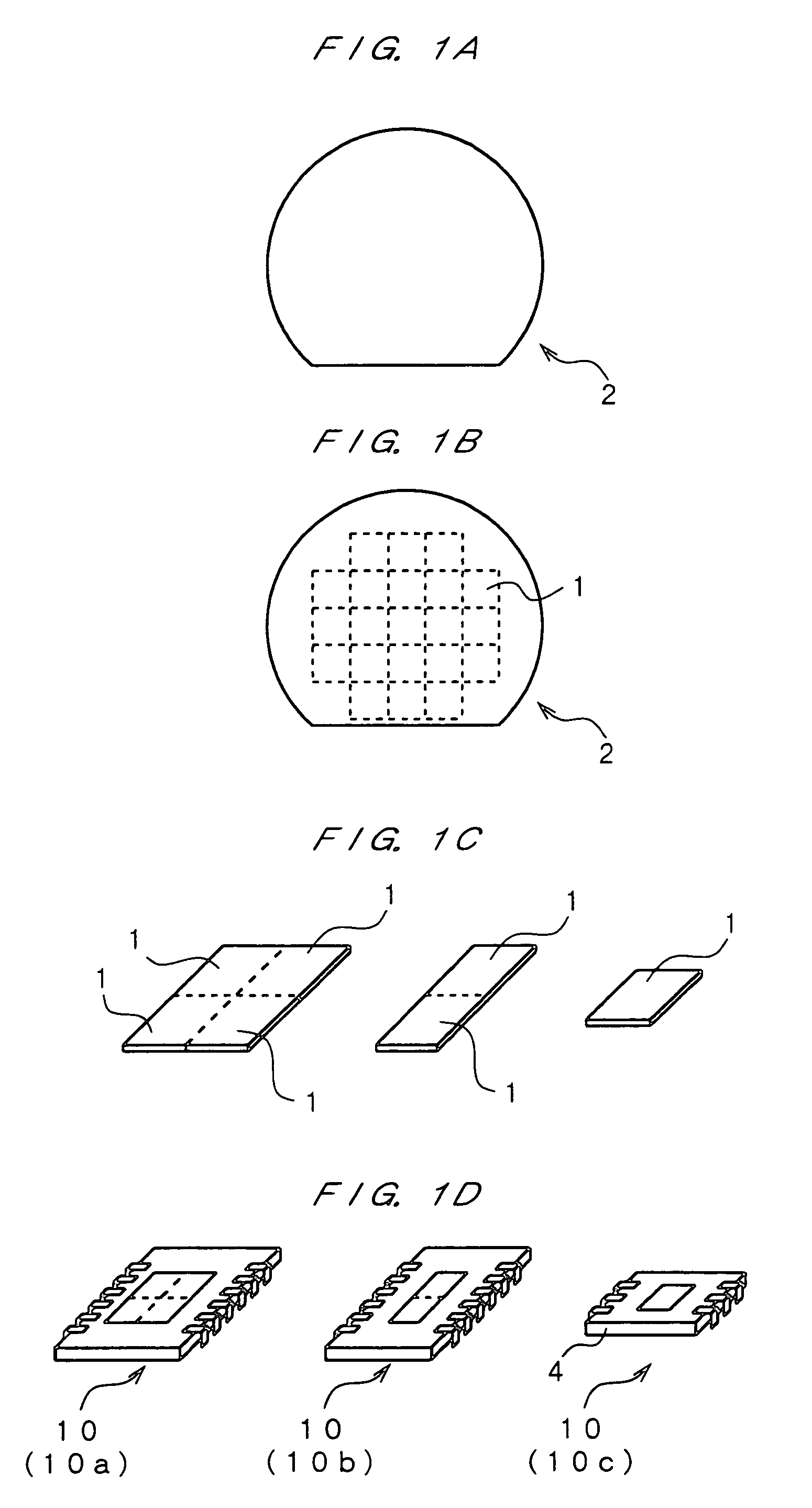
[0027]Next, the memory module of a second embodiment by an application of the present invention will be subsequently described. The memory module according to the present embodiment is fabricated by a chip size package mounting technique (CSP). FIGS. 4A to 4D are diagrams showing the fabrication procedure of the memory module according to the present embodiment.

[0028]First, as shown in FIGS. 4A and 4B, the semiconductor wafer 12 is introduced to form identical memory chips 11 on this semiconductor wafer 12 (the first step). A plurality of respective regions surrounded with a dotted line in FIG. 4B show a single unit (the minimum unit of dividing) of the memory chip 11 after CSP mounting. Next, for a whole of the semiconductor wafer 12 in the status of forming a plurality of memory chips 11, as shown in FIG. 4C, after conducting wiring and resin sealing, CSP mounting is carried out to form the terminal (the second step).

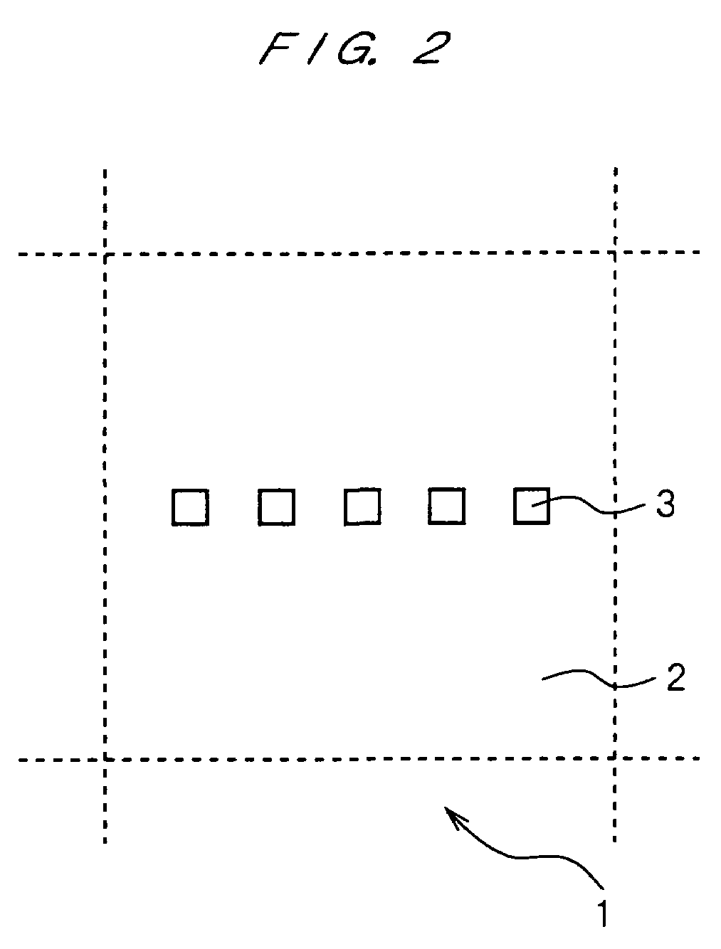
[0029]FIG. 5 is an enlarged sectional view of the memory chip 11...

first embodiment

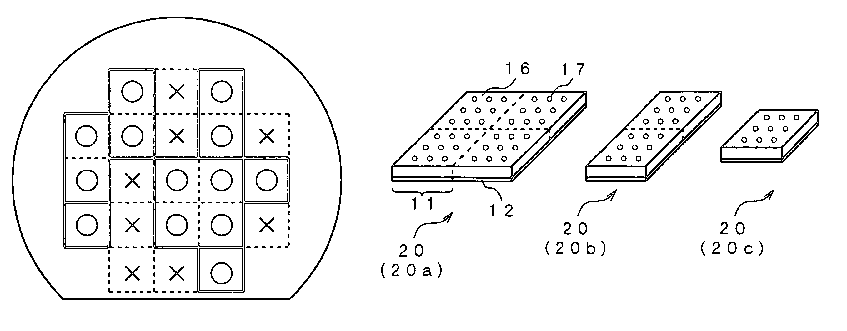
[0032]Subsequently, on the basis of a result of quality test in the third step, as shown in FIG. 4D, memory chips 11, which have been mounted by CSP and determined as good, are divided in the unit of one or a plurality (two or four pieces) of semiconductor chips and then, finally, either the memory module 20a having four memory chips 11 divided, the memory module 20b having two memory chips 11 divided, or the memory module 20c having one memory chip 11 divided is completed (a fourth step). Concretely, the dividing method shown in FIGS. 3A and 3B applied to the first embodiment described above is adopted.

[0033]As described above, after forming a plurality of identical memory chips 11 on the semiconductor wafer 12, the CSP mounting is carried out. Among respective memory chips 11 mounted by CSP, those only determined as good by a quality test are divided to fabricate the memory module 20 as the semiconductor device and thus, it does not take place that a part of defective memory chips...


PUM


Abstract

A semiconductor device and a method for manufacturing the semiconductor device mountable with high density, which includes a simplified process but is capable of reducing a defect rate. A plurality of identical memory chips are formed on a semiconductor wafer, and a go / no-go test is conducted on all the memory chips. The semiconductor wafer is cut and divided into pieces that each consists of one, or two, or four good memory chips, and they are mounted on a substrate to form a memory module.

Description

TECHNICAL FIELD[0001]The invention relates to a semiconductor device mounted on a memory substrate, a mother board, or the like and a method for manufacturing the same.BACKGROUND ART[0002]A semiconductor chip such as a memory chip cutout from a semiconductor wafer is generally mounted on a printed substrate or the like in a packaging condition. However, an outer size of a package is considerably larger than the size of a various types of the semiconductor chips themselves and therefore, there is a certain limit in the number of the packages mountable on the printed substrate or the like.[0003]On the other hand, recently, a multichip module (MCM), in which a plurality of semiconductor chips are mounted on the substrate, is being popularized. Using the multichip module allows the followings: (1) miniaturization of a mounting area and weight reduction accompanying with this, (2) realization of a high performance and high speed by high density wiring and bear chip mounting, and (3) keep...

Claims


Application Information

Patent Timeline
IPC IPC(8): G11C29/00H01L21/66H01L21/78
CPCG11C29/006H01L21/78H01L22/20H01L2924/014H01L2924/0002H01L2924/00
Inventor IKEDA, KOUICHIIKEDA, TAKESHI
Owner INVENSAS CORP
Why Eureka
Try Eureka