Lower electrode isolation in a double-wide trench and method of making same

a technology of low electrodes and trenches, which is applied in the direction of digital storage, semiconductor devices, instruments, etc., can solve the problems of conductive failure, increasing the incidence of ricochet of dopants instead of implantation, and becoming increasingly difficult to properly dope the matchstick structur

Inactive Publication Date: 2005-11-29
OVONYX MEMORY TECH LLC
View PDF2 Cites 33 Cited by
  • Summary
  • Abstract
  • Description
  • Claims
  • Application Information

AI Technical Summary

Problems solved by technology

One challenge of forming a lower electrode in a phase-change memory cell is to shrink the cell size while still being able to dope the polysilicon matchstick structure in an ever-increasing aspect ratio recess.
As the aspect ratio of the recess increases, it becomes increasingly difficult to properly dope the matchstick structure for at least two reasons.
First, an increasingly steep angle of implantation directed at the polysilicon wall will result in an increasingly higher incidence of ricochet of the dopants instead of implantation.
Second, as that aspect ratio gets higher, it becomes increasingly difficult to get dopant to strike the polysilicon wall at the bottom of the recess; an inadequate doping at the bottom results in a conductive failure.
Another challenge of forming a lower electrode in a phase-change memory cell is to shrink the cell size while not increasing capacitative coupling between a given memory cell and a contiguous memory cell.
Another process challenge is the singulation of the lower electrode film in order to achieve discrete conductive electrodes without decreasing process yield.
Another challenge for a phase-change memory device is power consumption required in setting and resetting memory material.
Power consumption is significant, particularly in portable devices such as a hand-held or wireless device.

Method used


Image

  • Lower electrode isolation in a double-wide trench and method of making same
  • Lower electrode isolation in a double-wide trench and method of making same
  • Lower electrode isolation in a double-wide trench and method of making same

Examples


Embodiment Construction

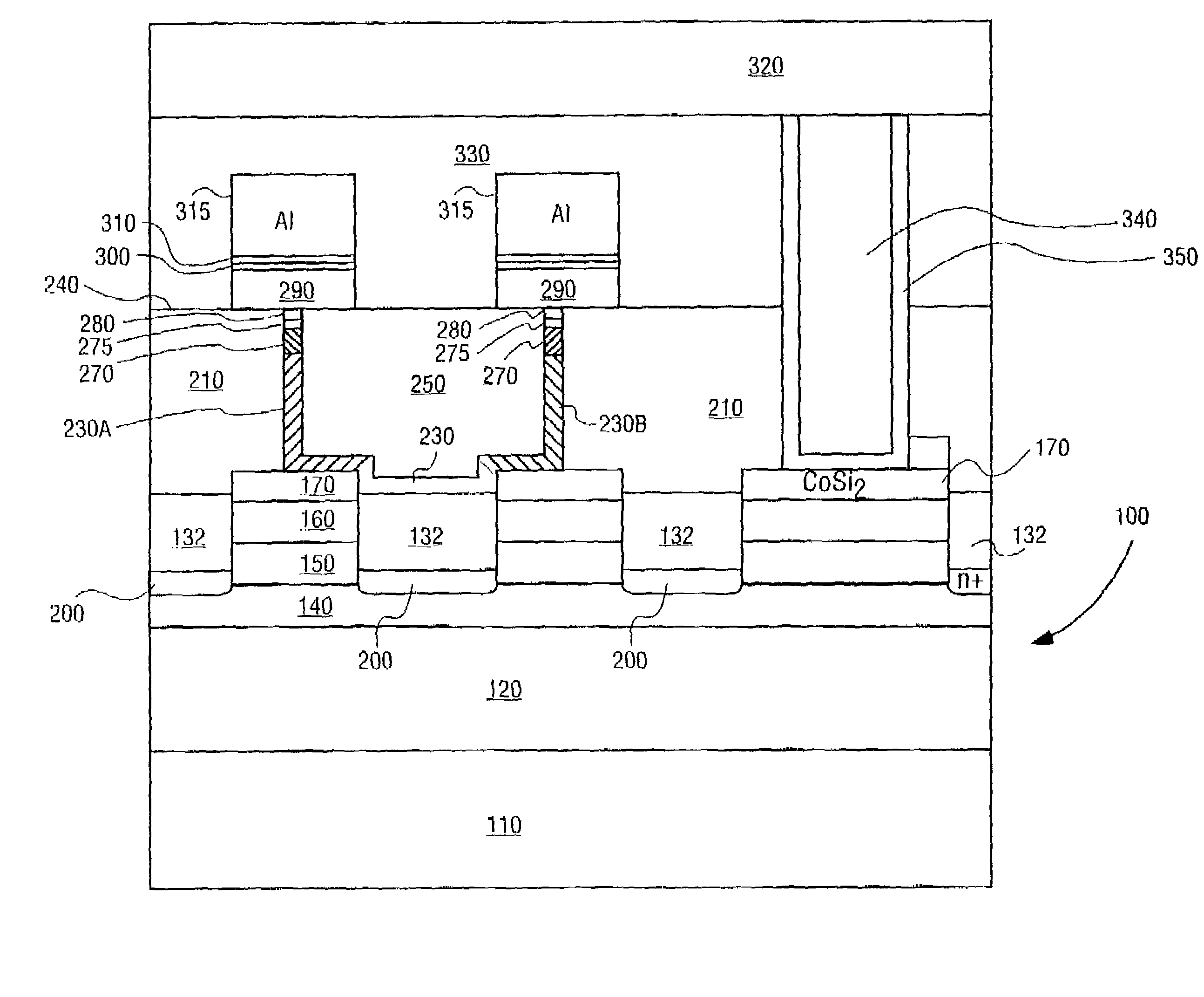
[0035]The invention relates to a memory device that is used with phase-change material to memorialize data storage. The device uses a lower electrode material that is referred to as a “matchstick”. Beneath the matchstick, an active area that may be a diode stack is provided to activate the lower electrode. A first isolation trench may be formed, followed by formation of a second isolation trench. The second isolation trench is orthogonal to the first isolation trench. The lower electrode is formed over the diode stack portion of the memory cell structure, and a volume of phase change memory material is disposed above the matchstick. Either a high resistivity metal compound may be used as the lower electrode, or a polysilicon compound may be used.

[0036]The following description includes terms, such as upper, lower, first, second, etc. that are used for descriptive purposes only and are not to be construed as limiting. The embodiments of an apparatus or article of the present inventio...


PUM


Abstract

The invention relates to a phase-change memory device. The device includes a double-wide trench into which a single film is deposited but two isolated lower electrodes are formed therefrom. Additionally a diode stack is formed that communicates to the lower electrode. Additionally, other isolated lower electrodes may be formed along a symmetry line that is orthogonal to the first two isolated lower electrodes. The present invention also relates to a method of making a phase-change memory device. The method includes forming two orthogonal and intersecting isolation structure s around a memory cell structure diode stack.

Description

[0001]This is a divisional of prior application Ser. No. 09 / 749,127, filed Dec. 26, 2000 now U.S. Pat. No. 6,646,297.BACKGROUND OF THE INVENTION[0002]1. Field of the Invention[0003]The present invention relates to a phase-change memory device. More particularly, the present invention relates isolation of an electrically conductive film in the memory device. In particular, the present invention relates to an undoped region in a double-wide lower electrode that spans two diode stacks in a phase-change memory device.[0004]2. Description of Related Art[0005]As microelectronic technology progresses, the need has arisen for new data retention schemes. One such data retention scheme is the chalcogenide phase-change technology. Typically, a phase-change memory device includes a polysilicon lower electrode, also known as a “matchstick”.[0006]One challenge of forming a lower electrode in a phase-change memory cell is to shrink the cell size while still being able to dope the polysilicon match...

Claims


Application Information

Patent Timeline
Patent Type & Authority Patents(United States)
IPC IPC(8): G11C8/02H01L27/24
CPCH01L45/06H01L45/1233H01L45/126H01L45/144H01L45/16H01L27/2409H01L27/2463H10B63/20H10B63/80H10N70/8413H10N70/231H10N70/011H10N70/826H10N70/8828
Inventor DENNISON, CHARLES
Owner OVONYX MEMORY TECH LLC
Why Eureka
Try Eureka