Method and circuit for generating single-sideband optical signal

a single-sideband optical signal and circuit technology, applied in optics, instruments, electrical equipment, etc., can solve the problems of difficult to realize chirpless optical phase modulators, 90-degree hybrid circuits that cannot operate over a wide frequency band, and inability to generate ssb optical signals, etc., to achieve excellent narrowband properties, reduce the effect of excess high frequency components

Active Publication Date: 2005-11-29
NAT INST OF INFORMATION & COMM TECH +2
View PDF8 Cites 42 Cited by
  • Summary
  • Abstract
  • Description
  • Claims
  • Application Information

AI Technical Summary

Benefits of technology

[0026]Accordingly, the present invention is made to overcome the above-mentioned disadvantages and it is an object of the present invention to provide a method for generating a single-sideband optical signal, whereby an SSB optical signal having excellent narrowband properties can be generated with a relatively simple configuration without a 90-degree hybrid circuit, and further, an excess high frequency component can be substantially eliminated.

Problems solved by technology

First, for microwaves, an SSB optical signal cannot be generated using a wideband baseband signal, which is generally used in optical communication.
However, the 90-degree hybrid circuit does not operate over a wide frequency band from a low frequency close to DC up to a high frequency.
Second, it is difficult to realize a chirpless optical phase modulator.
If such modulator can be realized, it prevents the realization of high-density multiplexing.
According to the foregoing methods, the SSB optical signal can be produced as mentioned above but undesirable components remain in the optical spectrum.

Method used


Image

  • Method and circuit for generating single-sideband optical signal
  • Method and circuit for generating single-sideband optical signal
  • Method and circuit for generating single-sideband optical signal

Examples


Embodiment Construction

[0048]To describe the present invention in detail, the invention will now be explained with reference to the accompanying drawings.

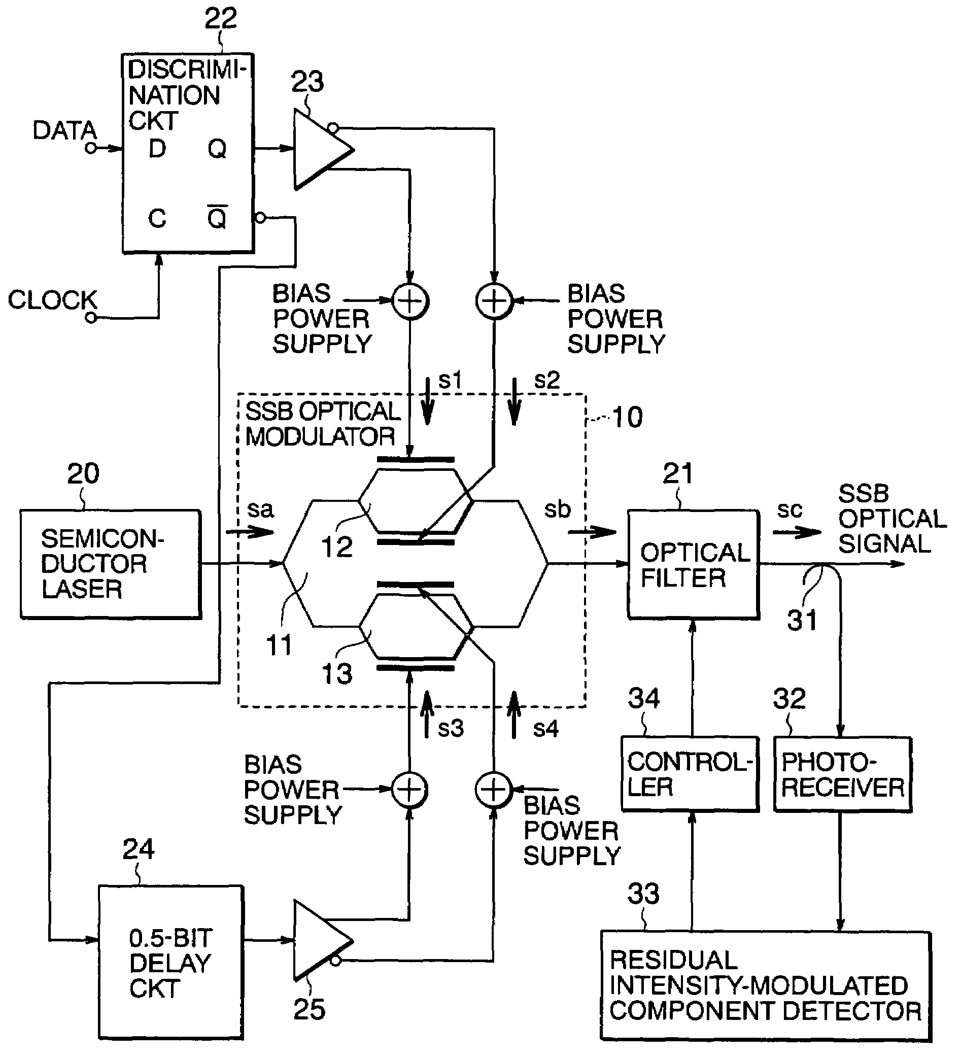
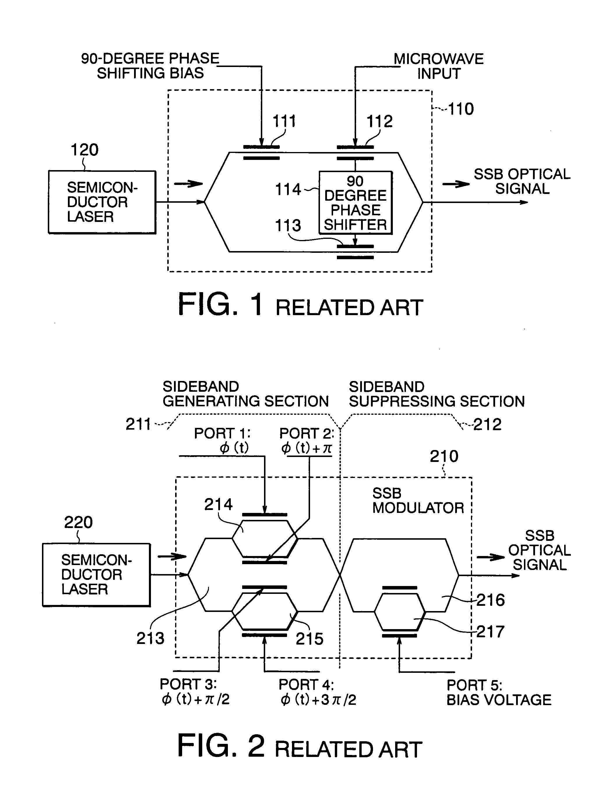
[0049]FIG. 6 is a diagram showing a circuit according to an embodiment of the present invention. In the circuit for generating a single-sideband optical signal shown in FIG. 6, a binary NRZ data signal is supplied to a transmitter having an SSB optical modulator 10 at a bit rate of 10 Gb / s. Carrier wave light Sa is generated from a semiconductor laser 20 having a wavelength of 1.55 μm. The light Sa is modulated by the SSB optical modulator 10 to obtain an SSB optical signal Sb. In this instance, the SSB optical modulator 10 includes the following components. Mach-Zehnder interferometers 12 and 13 for driving are integrated in both arms of a Mach-Zehnder interferometer 11 on a lithium niobate substrate. The lithium niobate substrate is used in the above-mentioned related art shown in FIG. 2.

[0050]Referring to FIG. 6, the transmitter further includes an op...


PUM

PropertyMeasurementUnit
wavelengthaaaaaaaaaa
frequencyaaaaaaaaaa

Abstract

The present invention relates to a method for generating a single-sideband optical signal. According to the method, as data signals having a 90-degree phase difference with respect to input data signals, which are NRZ signals at 10 Gb / s, 0.5-bit delay data signals are generated by a 0.5-bit delay circuit for obtaining a delay corresponding to π / 2 of the bit period of the input data signal. An SSB optical signal produced from the data signals and the 0.5-bit delay data signals is generated through an optical filter. Further, to eliminate a residual intensity-modulated component, the generated SSB optical signal is fed back to appropriately adjust the center frequency of the optical filter. The carrier output frequency of a semiconductor laser can be adjusted instead of the center frequency of the optical filter. When an RZ signal is used as an input data signal, a 0.25-bit delay circuit is used.

Description

BACKGROUND OF THE INVENTION[0001]1. Field of the Invention[0002]The present invention relates to a method and circuit for generating a single-sideband optical signal in optical fiber communication employing a single-sideband (SSB) optical modulation system. More particularly, the present invention relates to a method and circuit for generating a single-sideband optical signal without necessitating a 90-degree hybrid circuit.[0003]2. Description of the Related Art[0004]To increase the transmission capacity of an optical-fiber communication system, the use of wavelength division multiplexing (WDM) together with the realization of higher bit rates is effective. Following several WDM optical transmission systems have recently been put into practical use. According to one of these systems, an optical signal having a bit rate of 10 Gb / s per wavelength is wavelength-multiplexed at a frequency interval of 50 GHz (corresponding to a wavelength interval of 0.4 nm in a waveband of 1.55 μm), an...

Claims


Application Information

Patent Timeline
Patent Type & Authority Patents(United States)
IPC IPC(8): G02F1/035H04B10/00H04B10/516H04B10/61
CPCH04B10/505H04B10/50572
Inventor ONO, TAKASHISHIMOTSU, SHINICHIIZUTSU, MASAYUKI
Owner NAT INST OF INFORMATION & COMM TECH
Why Eureka
Try Eureka