Multilayered circuit board forming method and multilayered circuit board

a technology of multi-layer circuit boards and forming methods, applied in resist details, conductive pattern formation, chemistry apparatus and processes, etc., can solve the problems of difficult to accurately form electronic circuits, insufficient treatment to eliminate such occurrences, and extreme deformation of electrical characteristics of electronic circuits, etc., to achieve easy control of positional accuracy and accuracy. high, the effect of high quality

Inactive Publication Date: 2005-12-06
PANASONIC CORP
View PDF12 Cites 2 Cited by
  • Summary
  • Abstract
  • Description
  • Claims
  • Application Information

AI Technical Summary

Benefits of technology

[0024]The purpose of the present invention is to solve the above drawbacks. An object of the present invention is to provide a multilayered circuit board with high accuracy and quality, and a method of forming such a multilayered circuit

Problems solved by technology

Therefore, such patchy printing extremely degrades an electrical characteristic of electronic circuits as designed.
However, this treatment is not sufficient to eliminate such occurrence, particularly noticeable at the above-stated concave/convex portion 5.
For this reason, as the number of layers is increased, it becomes difficult to accurately form electronic circuits.
Regarding these two types of accuracy, if dimensional and positional deviations are inadequately controlled, these deviations are accumulated as the number of circuit boards to be connected is increased, thereby inconveniently limiting a number of circuit board laminations and, at worst, making it impossible to perform a connecting process itself.
Even with these deviations in accuracy being adequately controlled, the above-mentioned inconveniences occur if a positional relationship among the circuit boards is changed through a heating and pressuring process.
This tends to cause positional deviations among the layers.
Moreover, a hole-making operation for preparing a via hole takes a lot of time and processes, thereby causing an increase in the number of processes required in this scheme.
Therefore, the above-mentioned problems in the connective formation scheme, such as high accuracy in terms of position among the circuit board and an increase in the number of processes in order to make a hole for preparing a via hole, do not occur.
Furthermore, the larger the number of layers of circuit boards, the larger the number and size

Method used


Image

  • Multilayered circuit board forming method and multilayered circuit board
  • Multilayered circuit board forming method and multilayered circuit board
  • Multilayered circuit board forming method and multilayered circuit board

Examples


first embodiment

[0036

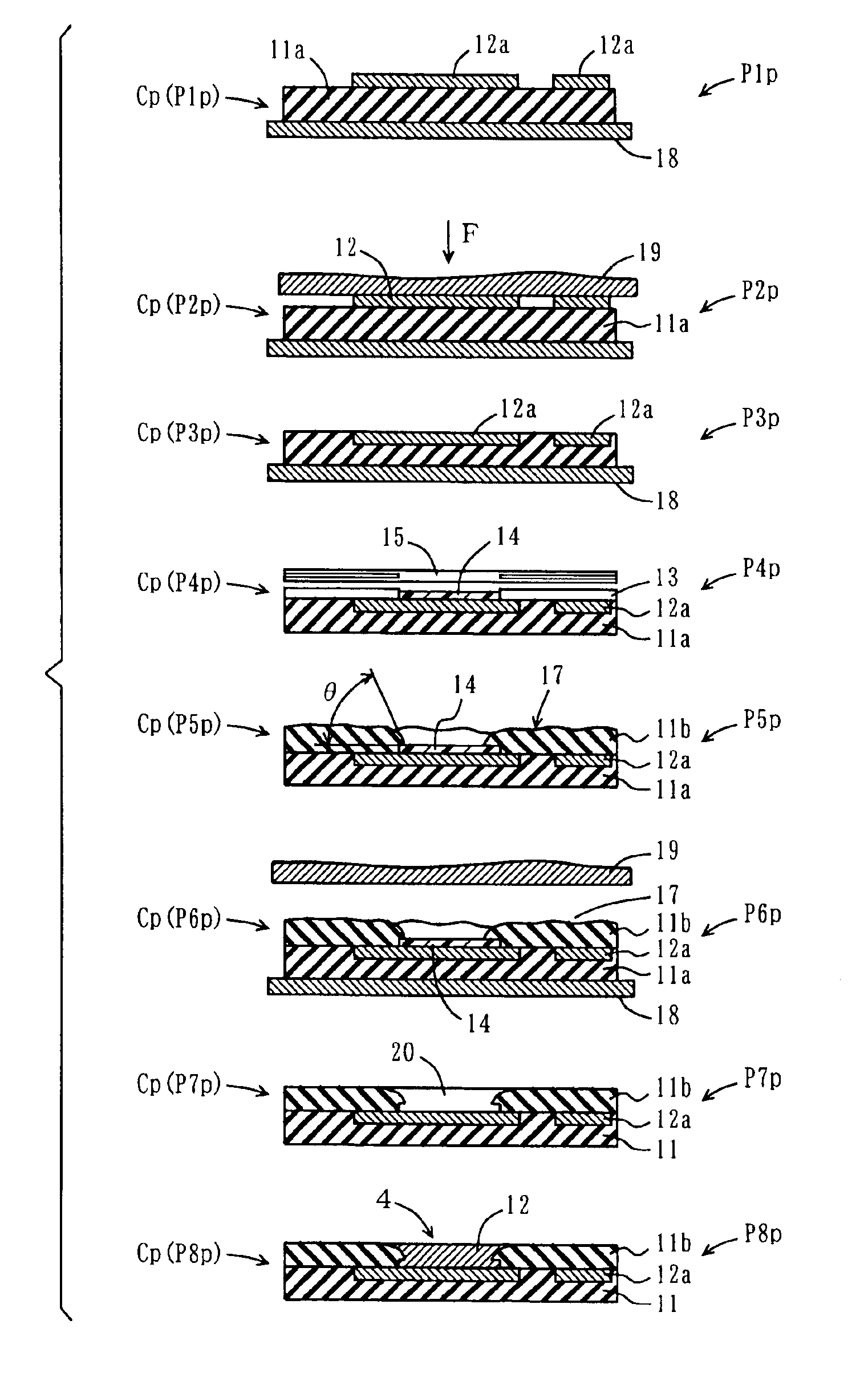
[0037]With reference to FIG. 1, a method of forming a multilayered circuit board according to a first embodiment of the present invention is described below. A multilayered circuit board MS1 according to the present invention is formed by using a screen printing scheme as in the above-described conventional successive formation scheme.

[0038]FIG. 1 illustrates a procedure of successively forming circuit boards one by one starting from a circuit board of a first layer by using a screen printing scheme, the procedure including processes P1p, P2p, P3p, P4p, P5p, P6p, P7p, and P8p shown stepwise. For convenience in description, circuit boards corresponding to these processes are hereinafter referred to as a circuit board CP(P1p), a circuit board CP(P2p), a circuit board CP(P3p), a circuit board CP(P4p), a circuit board CP(P5p), a circuit board CP(P6p), a circuit board CP(P7p), and a circuit board CP(P8p), respectively.

[0039]In process P1p, an insulating board 11a, which forms a circ...

second embodiment

[0059

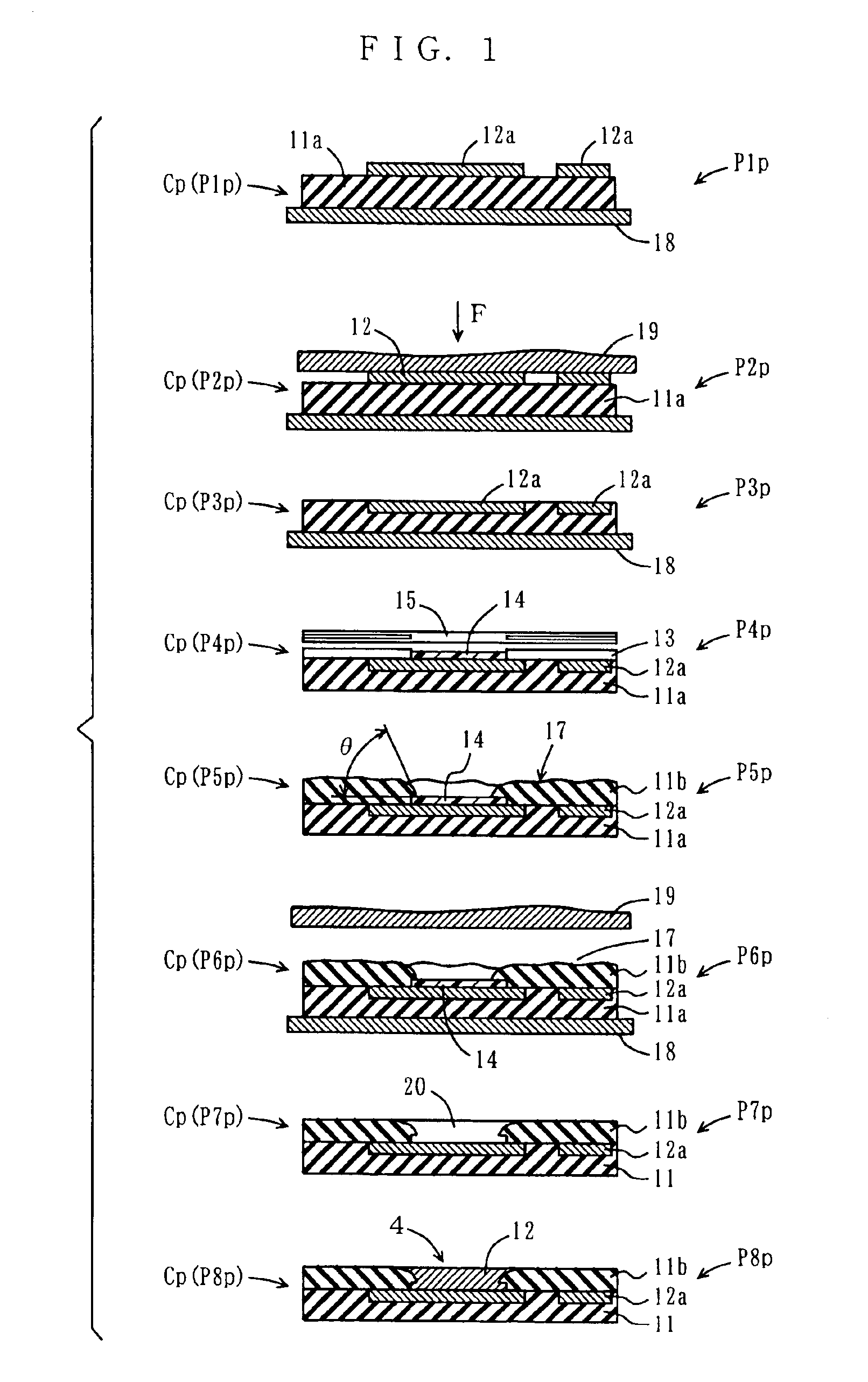
[0060]With reference to FIGS. 2 and 3, a scheme is described below for alternately printing a conductor and an insulating layer on an insulating board to form a multilayered circuit board. FIG. 2 is a cross section of a multilayered circuit board MS2 according to a second embodiment. FIG. 3 schematically illustrates a procedure of forming the multilayered circuit board MS2.

[0061]As illustrated in FIG. 2, the multilayered circuit board MS2 is formed by layering five insulating boards 11-1, 11-2, 11-3, 11-4 and 11-5, each having mounted thereon electric circuits. Here, components, a heating and pressuring scheme, and conditions thereof used in the present embodiment are basically the same as those described in the first embodiment, and therefore are not described herein unless otherwise particularly required.

[0062]As illustrated in FIG. 3, first prepared in process P1p-1a is the insulating board 11-1 formed of a sheet or a film containing a plastic element, such as a polyester re...

third embodiment

[0073

[0074]With reference to FIG. 4, a scheme is described below for forming a multilayered circuit board incorporated with a component, such as a semiconductor, a resistor, a capacitor, and a coil. FIG. 4 schematically illustrates a procedure of forming a multilayered circuit board MS3 according to a third embodiment. Here, components, a heating and pressuring scheme, and conditions thereof used in the present embodiment are basically the same as those described in the first and second embodiments, and therefore are not described herein unless otherwise particularly required.

[0075]In process P1p-b, an insulating board 11-a formed by the scheme according to the first or second embodiment, and embedded with conductor 12a for forming electronic circuits are provided together with a semiconductor device 31 having bumps 32 formed at an electrode portion. The semiconductor device 31 is placed at a predetermined location on the insulating board 11-a so that a side where the bumps 32 of th...


PUM

PropertyMeasurementUnit
Temperatureaaaaaaaaaa
Pressureaaaaaaaaaa
Surfaceaaaaaaaaaa

Abstract

A multilayered circuit board and a method of forming the multilayered circuit board are provided. In a first circuit forming process, a first circuit is formed on an insulating board with a conductor; in a circuit embedding process, the first circuit is embedded in the insulating board so as to have a predetermined surface flatness and a predetermined parallelism; in a masking process, a pilot hole for a via hole is masked at a part of a surface of the circuit; in an insulating layer forming process P5p, an insulating material is applied as a layer to the surface except that portion thereof covered by the mask; in an insulating material layer flattening process, the surface of the insulating material layer is flattened so as to have the predetermined surface flatness and the predetermined parallelism; and in a pilot hole forming process, the mask is removed.

Description

BACKGROUND OF THE INVENTION[0001]1. Field of the Invention[0002]The present invention relates to a multilayered circuit board formed by layering electric circuits each having electronic components mounted thereon, and a method of forming such a multilayered circuit board.[0003]2. Description of the Background Art[0004]With reference to FIGS. 5, 6, and 7, conventional schemes used for forming a multilayered circuit board are described below. These schemes can be broadly classified in two categories, which are hereinafter referred to as a connective formation scheme and a successive formation scheme.[0005]In the connective formation scheme, a desired number of circuit boards prepared in advance are layered so as to be connected to each other, thereby forming a multilayered circuit board.[0006]In the successive formation scheme, one circuit board is first formed, on which another circuit board is then formed. Repeating this process forms a multilayered circuit board with a desired numb...

Claims


Application Information

Patent Timeline
IPC IPC(8): H05K3/46H05K3/00
CPCH05K3/0017H05K3/002H05K3/0041H05K3/4644H05K2201/0179H05K2201/0376Y10T29/49155H05K2203/0582Y10T29/49165Y10T29/49117Y10T29/49126Y10T29/4913H05K2203/0278H05K3/46
Inventor NISHIKAWA, KAZUHIROTSUKAHARA, NORIHITOOTANI, HIROYUKI
Owner PANASONIC CORP
Why Eureka
Try Eureka