High voltage, high temperature capacitor and interconnection structures

a capacitor and high-temperature technology, applied in the direction of fixed capacitor details, fixed capacitors, semiconductor/solid-state device details, etc., can solve the problems of limiting the operation of the device, the physical and operating characteristics of the device become limited by the characteristics of the insulator rather than those of silicon carbide, and the tendency of silicon dioxide to electrically break down, etc., to achieve a high mean time to failure

Inactive Publication Date: 2005-12-06
CREE INC
View PDF78 Cites 33 Cited by
  • Summary
  • Abstract
  • Description
  • Claims
  • Application Information

AI Technical Summary

Benefits of technology

[0027]Embodiments of the present invention may also provided a high mean time to failure interconnection structure for an integrated circuit having a plurality of semiconductor devices in a silicon carbide substrate, an insulating layer on the plurality of semiconductor devices and a first interconnect layer having a plurality of regions of interconnection metal on the insulating layer opposite the plurality of semiconductor devices. A layer of dielectric material is provided on the first layer of oxide opposite the first interconnect layer and a second interconnect layer is provided on the layer of dielectric material opposite the first interconnect layer and having a plurality of regions of interconnection metal. The layer of dielectric material is silicon oxynitride having a formula Si3N4-xOx, where 0<X≦1;

Problems solved by technology

For power devices, the main concerns include the absolute values of power that the device can (or must) handle, and the limitations on the device's operation that are imposed by the characteristics and reliability of the materials used.
By incorporating the insulating material, however, some of the physical and operating characteristics of the device become limited by the characteristics of the insulator rather than by those of silicon carbide.
Nevertheless, at high temperatures or high fields or both, at which the silicon carbide could otherwise operate satisfactorily, the silicon dioxide tends to electrically break down; i.e., to develop defects, including traps that can create a current path from the gate metal to the silicon carbide.
Stated differently, silicon dioxide becomes unreliable under the application of high electric fields or high temperatures (250°-400° C.) that are applied for relatively long time periods; i.e., years and years.
Additionally, those familiar with the characteristics of semiconductors and the operation of semiconductor devices will recognize that passivation also represents a challenge for structures other than insulated gates.
Such an oxide layer can suffer all of the disadvantages noted above under high field or high temperature operation.
Accordingly, IGFET devices formed in silicon carbide using silicon dioxide as the insulator tend to fall short of the theoretical capacity of the silicon carbide because of the leakage and the potential electrical breakdown of the silicon dioxide portions of the device.
Although other candidate materials are available for the insulator portion of silicon carbide IGFETs, they tend to have their own disadvantages.
Other materials have poor quality crystal interfaces with silicon carbide and thus create as many problems (e.g., traps and leakage current) as might solved by their high dielectric constant.
Others such as tantalum pentoxide (Ta2O5) and titanium dioxide (TiO2) tend to exhibit an undesired amount of leakage current at higher temperatures.
Thus, simply substituting other dielectrics for silicon dioxide presents an entirely new range of problems and disadvantages in their own right.
Recent attempts to address the problem have included the techniques described in U.S. Pat. No. 5,763,905 to Harris, “Semiconductor Device Having a Passivation Layer.” Harris '905 appears to be somewhat predictive, however, and fails to report any device results based on the disclosed structures.
Accordingly, such capacitors typically are desired to have a mean time to failure (MTTF) of 107 for a stress condition of, for example, as high as 200 volts at temperatures of up to about 300° C. Unfortunately, these extreme fields and temperatures may cause a conventional silicon nitride MIM capacitor to suffer from excessive leakage current and / or poor reliability (e.g. MTTF of about 200 hours).

Method used


Image

  • High voltage, high temperature capacitor and interconnection structures
  • High voltage, high temperature capacitor and interconnection structures
  • High voltage, high temperature capacitor and interconnection structures

Examples


Embodiment Construction

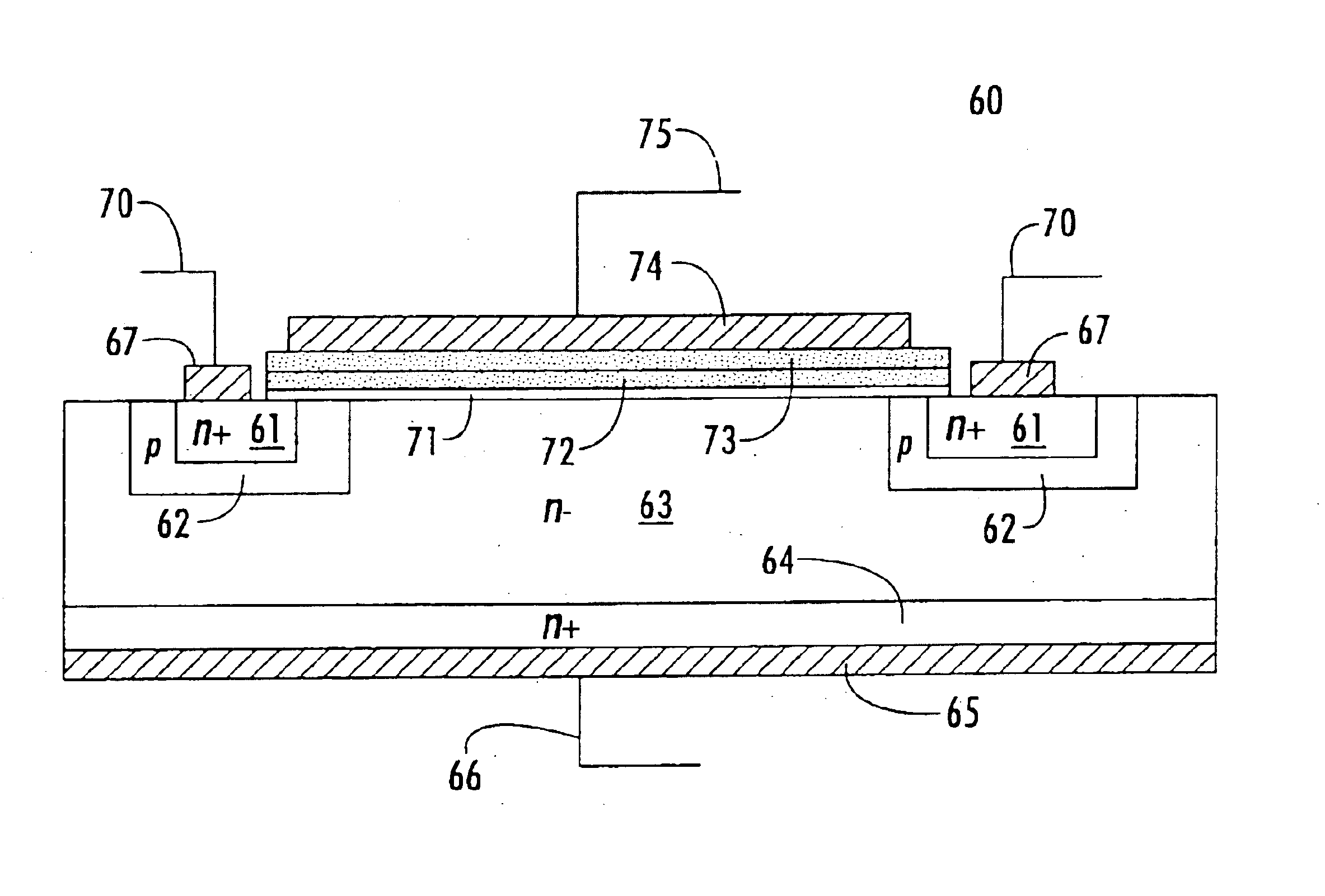
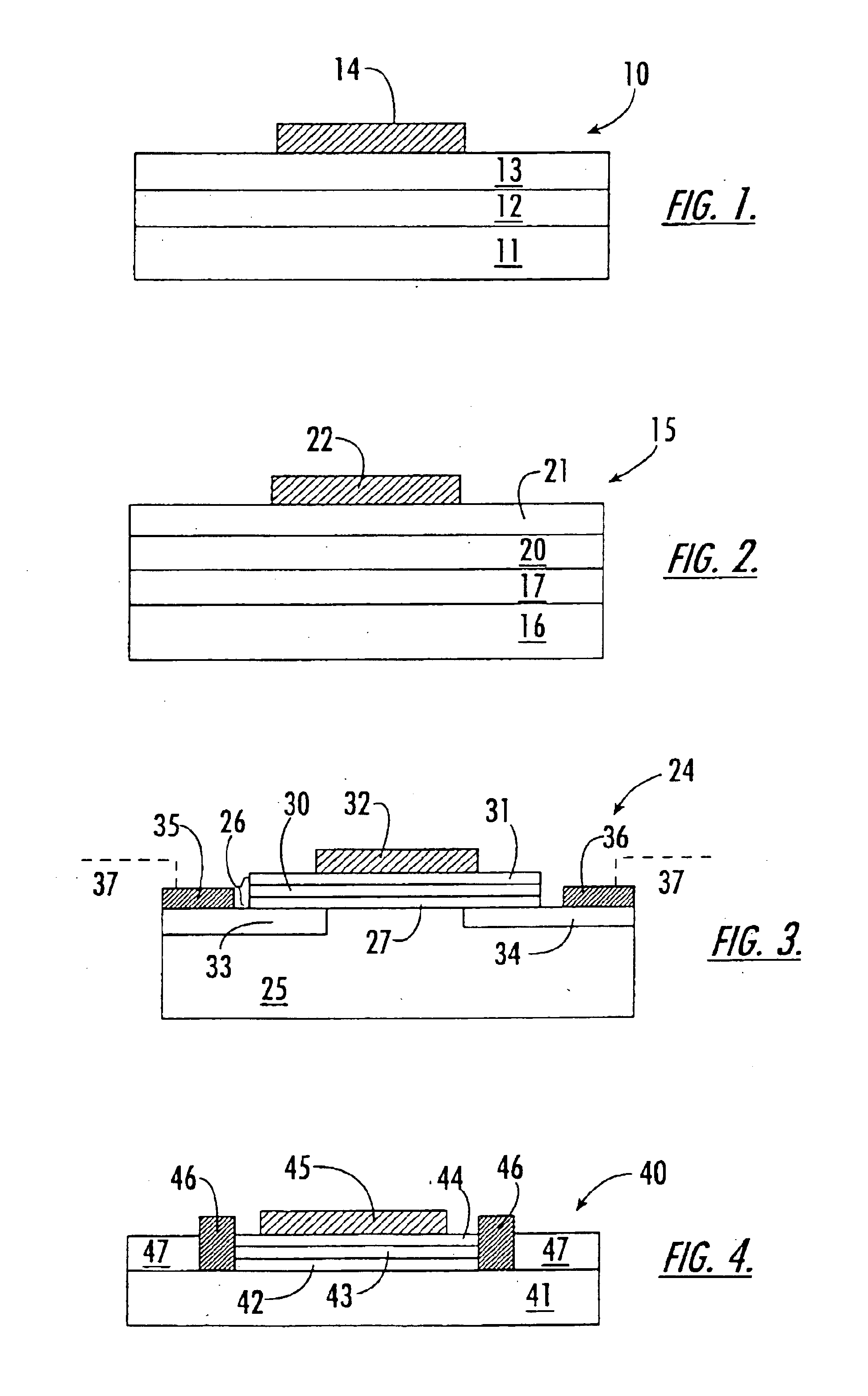
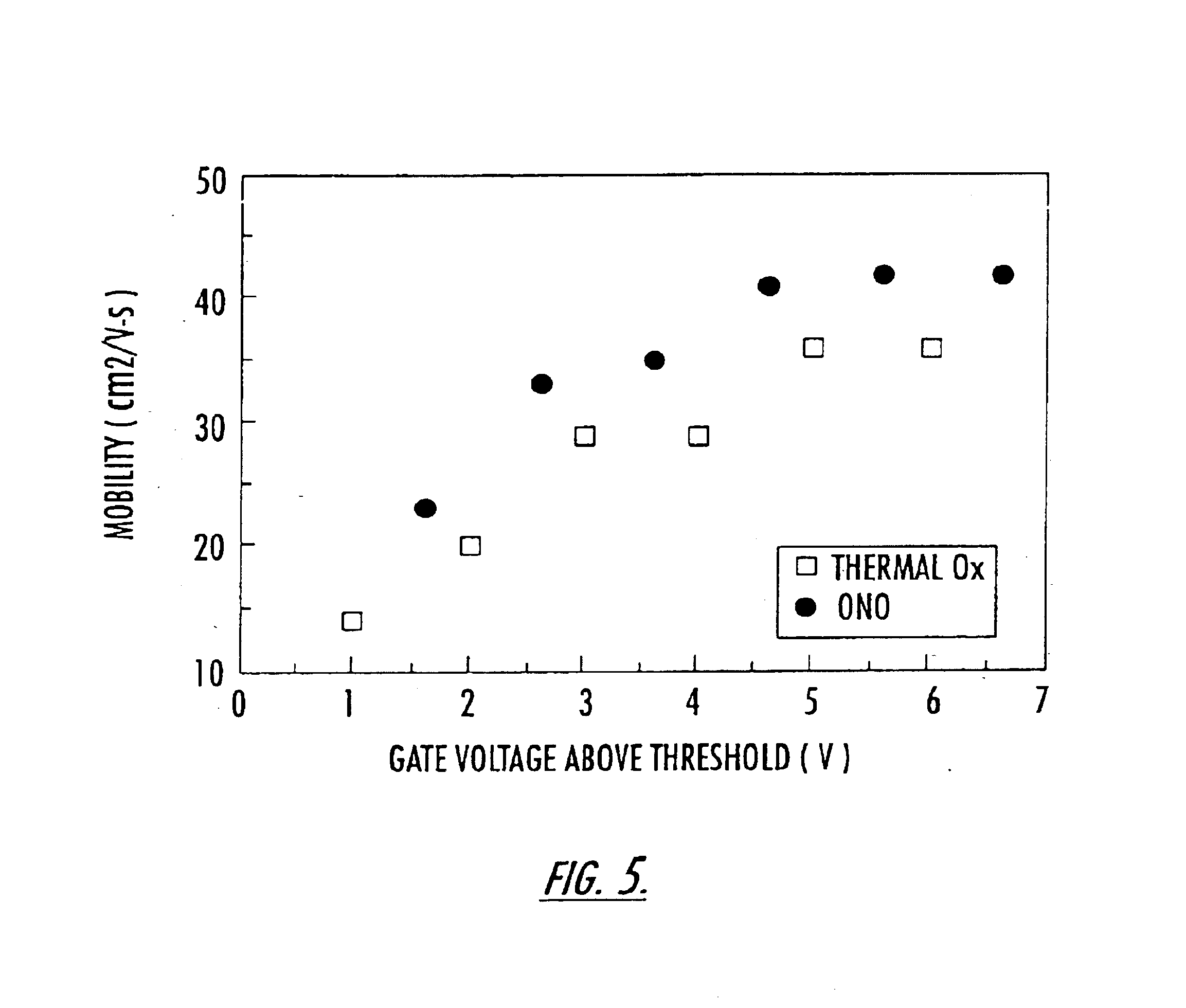
[0045]The present invention now will be described more fully hereinafter with reference to the accompanying drawings, in which preferred embodiments of the invention are shown. This invention may, however, be embodied in many different forms and should not be construed as limited to the embodiments set forth herein; rather, these embodiments are provided so that this disclosure will be thorough and complete, and will fully convey the scope of the invention to those skilled in the art. As illustrated in the Figures, the sizes of layers or regions are exaggerated for illustrative purposes and, thus, are provided to illustrate the general structures or the present invention. Like numbers refer to like elements throughout. It will be understood that when an element such as a layer, region or substrate is referred to as being “on” another element, it can be directly on the other element or intervening elements may also be present. In contrast, when an element is referred to as being “dir...


PUM

PropertyMeasurementUnit
thicknessaaaaaaaaaa
thicknessaaaaaaaaaa
temperatureaaaaaaaaaa

Abstract

Capacitors and interconnection structures for silicon carbide are provided having an oxide layer, a layer of dielectric material and a second oxide layer on the layer of dielectric material. The thickness of the oxide layers may be from about 0.5 to about 33 percent of the thickness of the oxide layers and the layer of dielectric material. Capacitors and interconnection structures for silicon carbide having silicon oxynitride layer as a dielectric structure are also provided. Such a dielectric structure may be between metal layers to provide a metal-insulator-metal capacitor or may be used as a inter-metal dielectric of an interconnect structure so as to provide devices and structures having improved mean time to failure. Methods of fabricating such capacitors and structures are also provided.

Description

RELATED APPLICATIONS[0001]The present application is a continuation-in-part of and claims priority from U.S. patent application Ser. No. 09 / 141,795 entitled “LAYERED DIELECTRIC ON SiC SEMICONDUCTOR STRUCTURES” filed Aug. 28, 1998, now U.S. 6,246,076 the disclosure of which is incorporated herein by reference as if set forth fully.STATEMENT OF GOVERNMENT INTEREST[0002]The present invention was developed with Government support under contract number DAAL01-98-C-0018 awarded by Army Research Laboratories and contract numbers N00014-99-C-0172 and N00014-99-C-0173 awarded by the United States Office of Naval Research. The Government has certain rights in this invention.FIELD OF THE INVENTION[0003]The present invention relates to high power, high field, or high temperature capacitive structures and in particular relates to capacitors and inter-metal dielectrics.BACKGROUND OF THE INVENTION[0004]For electronic devices, particularly power devices, silicon carbide offers a number of physical,...

Claims


Application Information

Patent Timeline
Patent Type & Authority Patents(United States)
IPC IPC(8): H01L29/749H01G4/33H01L21/02H01L21/04H01L21/28H01L21/314H01L21/329H01L21/336H01L21/338H01L21/822H01L27/04H01L27/08H01L29/06H01L29/12H01L29/161H01L29/24H01L29/40H01L29/51H01L29/739H01L29/78H01L29/812H01L29/861H01L29/94
CPCH01L21/045H01L29/94H01L27/0805H01L28/40H01L29/408H01L29/513H01L29/517H01L29/518H01L29/6606H01L29/66068H01L29/78H01L29/7802H01L29/8611H01L21/049H01L29/1608H01G4/33H01G4/1272H01G4/20H10B12/00
Inventor DAS, MRINAL KANTILIPKIN, LORI A.PALMOUR, JOHN W.SHEPPARD, SCOTTHAGLEITNER, HELMUT
Owner CREE INC
Why Eureka
Try Eureka