Semiconductor device with malfunction control circuit and controlling method thereof

a technology of malfunction control circuit and semiconductor device, which is applied in the field of semiconductor device integrated circuit having a chip malfunction control circuit, can solve the problems of difficult identification of repaired chips, user's inability to favor the repair of chips, and requirement that they be furnished with chips, so as to reduce production costs, protect business reputation, and simplify the burden on manufacturers to manage defective chips

Inactive Publication Date: 2005-12-06
SAMSUNG ELECTRONICS CO LTD
View PDF13 Cites 2 Cited by
  • Summary
  • Abstract
  • Description
  • Claims
  • Application Information

AI Technical Summary

Benefits of technology

[0014]Therefore, it is an object of the present invention to provide an integrated circuit of a semiconductor device for essentially prohibiting a defective chip from performing any operations.
[0015]It is another object of the present invention to provide a method of an integrated circuit of a semiconductor device for preventing a defective chip, which can not be repaired, from performing its normal operations in the manufacturing processes or even after its final product is placed in the market.
[0016]It is still another object of the present invention to provide a semiconductor memory device and its chip malfunction controlling method for reducing a manufacturer's burden of strict management with defective chips, for preventing any possible damage on its production cost and business image.
[0017]It is further another object of the present invention to provide a semiconductor memory or non-memory device and its chip malfunction controlling method for practically preventing a defective chip, which can not be repaired, from being approved for final sale to a consumer, even if wafer level defective chips may be sold or provided to the second producers.
[0020]According to the semiconductor device and the chip malfunction controlling method thereof, the defective chips, which cannot be repaired, are permanently prohibited from performing their normal operations in the following manufacturing processes or even after final products made of the defective chips are introduced into the market. This simplifies the burden on manufacturers to manage the defective chips, which reduces the production cost and can protect the business's reputation.

Problems solved by technology

On the other hand, some users do not favor the repaired chips.
Their demand for a highly reliable integrated circuit usually leads to a requirement that they not be furnished with chips that were originally identified as defective, and have subsequently been repaired.
Accordingly, the aforementioned circuit makes it difficult for a repaired chip to be identified.
If a chip determined as defective is incorrectly evaluated and assembled as a non-defective chip in the semiconductor device, it may not properly perform its functions, and may cause a fatal operational failure in the entire system.
There is a problem in the prior art in that a defective chip may be allowed to perform its normal operations in the manufacturing process that follows, or even after a final product made of the defective chip is introduced into the market.
Indeed, the process for hiding from the end user the fact that a chip has been repaired may also hide it from the manufacturer.
Indeed, as chips become incorporated in larger devices, the devices may malfunction from the defect.

Method used


Image

  • Semiconductor device with malfunction control circuit and controlling method thereof
  • Semiconductor device with malfunction control circuit and controlling method thereof
  • Semiconductor device with malfunction control circuit and controlling method thereof

Examples


Embodiment Construction

[0030]Objects and aspects of the present invention will become apparent from the following detailed description of a preferred embodiment with reference to the accompanying drawings. It should be noted that the same or similar reference numerals are used for the same or similar parts in the drawings for conveniences in description and understandings.

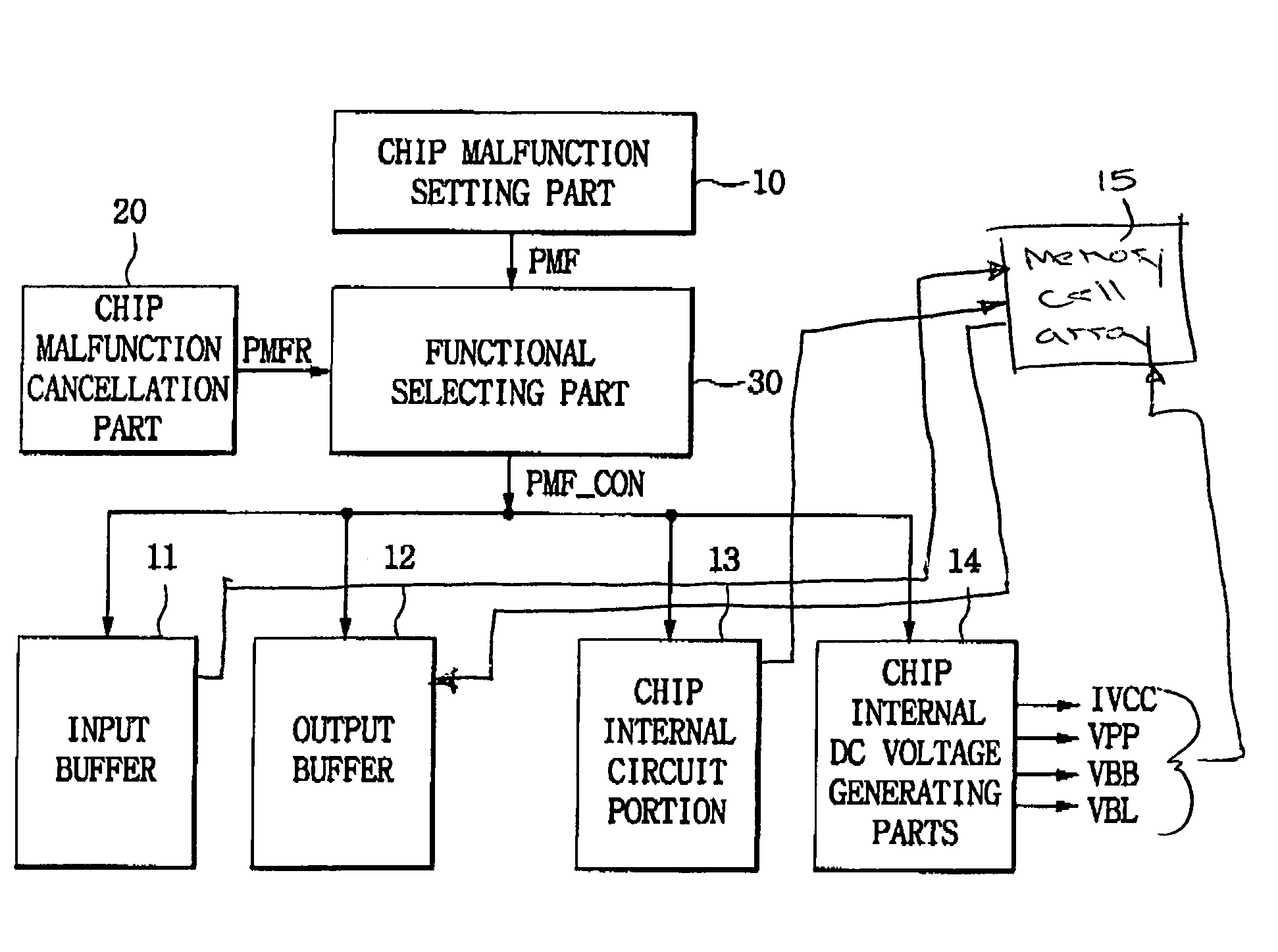
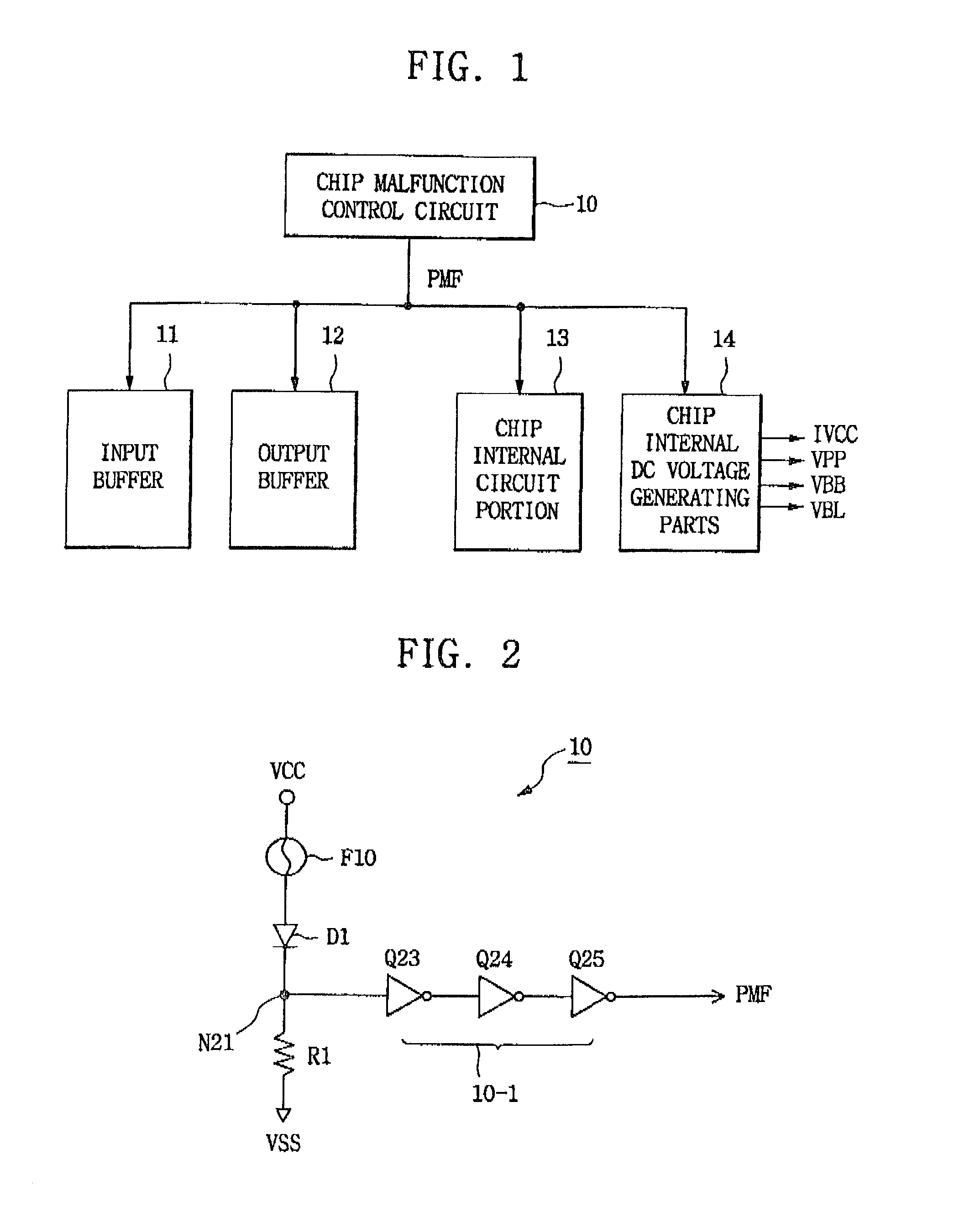
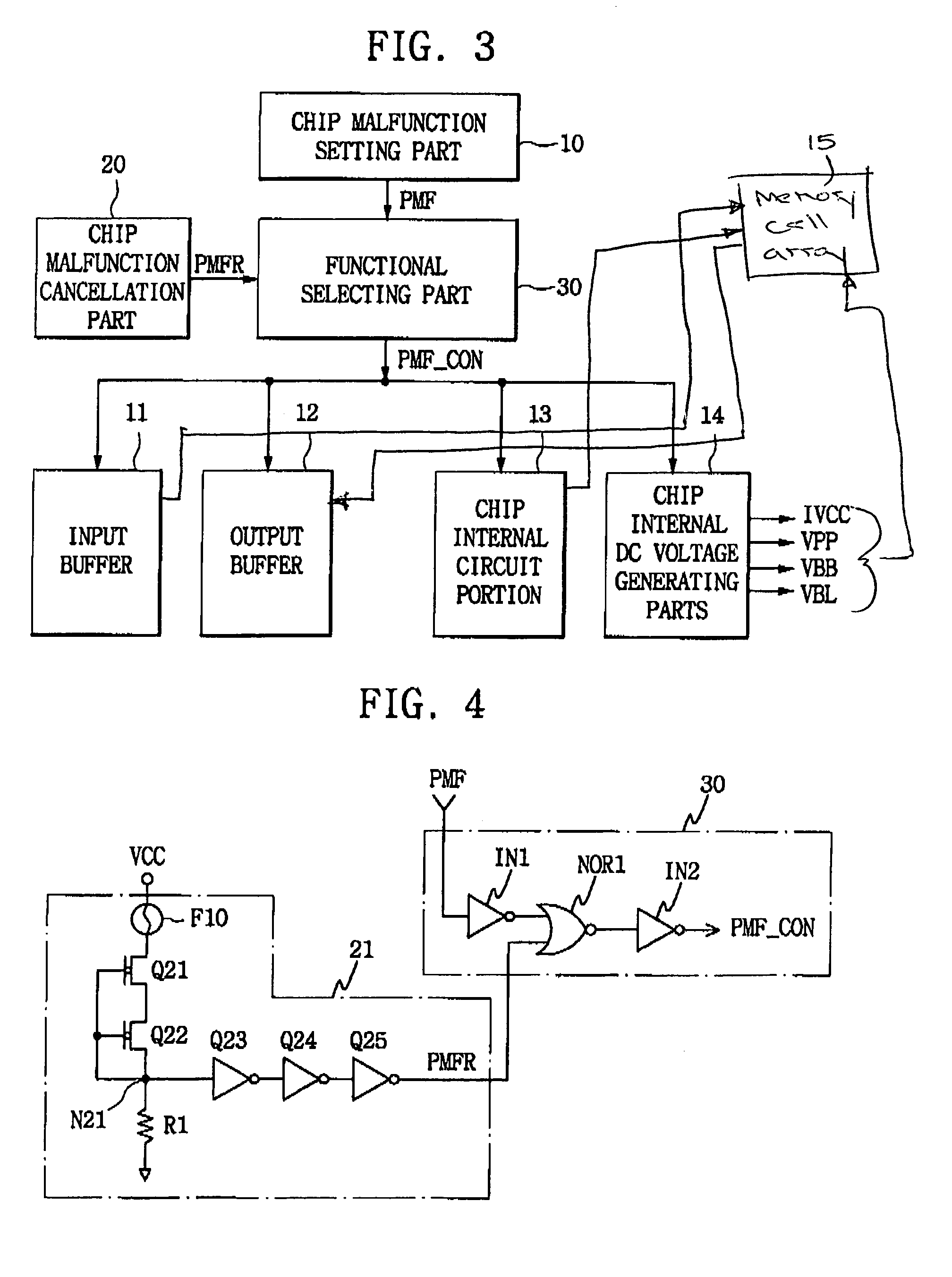
[0031]FIG. 1 is a block diagram for illustrating a semiconductor device having a chip malfunction controlling circuit in accordance with an embodiment of the present invention. A potential signal PMF (or also called a status signal) supplied from the chip malfunction controlling circuit 10 is applied to an input buffer 11, an output buffer 12, a chip internal circuit part 13 and a chip internal DC voltage generating part 14, which may be interconnected therebetween. At this time, the potential signal can be provided to at least one of those blocks of the input buffer 11, the output buffer 12, the chip internal circuit part 13 and the chi...


PUM


Abstract

An integrated circuit of a semiconductor device has a chip malfunction controlling circuit embedded in a chip. The circuit comprises a fusing part, to which a cutting will be made in the manufacturing process according to the result of the discrimination of a defect in a chip, with one end thereof being connected to a first power terminal. A signal generating part is connected to the other end of the fusing part, and to a second power terminal. The signal generating part generates a discrimination signal of discriminating whether the chip is defective or not, by whether the fusing part has been cut or not. The discrimination signal is supplied to at least one internal function circuit, and inhibits its operation if the fusing part has been cut. Furthermore, the chip malfunction controlling method comprises generating a discrimination signal that has a first state if a test fuse has been cut and a second state if the test fuse has not been cut. Then the discrimination signal is applied to the chip internal function circuits, to inhibit their operation if the fuse has been cut.

Description

CROSS REFERENCE TO RELATED APPLICATIONS[0001]This application claims priority from Korean Priority Document No. 99-23426, filed on Jun. 22, 1999 with the Korean Industrial Property Office, which document is hereby incorporated by reference. This application is a continuation-in-part of U.S. patent application Ser. No. 09 / 597,792 now abandoned, and claims the benefit of the filing date of that application.BACKGROUND OF THE INVENTION[0002]1. Field of the Invention[0003]The present invention relates to a semiconductor device, and more particularly to an integrated circuit of a semiconductor device having a chip malfunction controlling circuit, and a method for inhibiting operation of the components of a chip that was formerly deemed defective.[0004]2. Description of the Prior Art[0005]In general, semiconductor device manufacturers carry out an electrical test to all chips, to check that an integrated circuit of wafer level chip or package level chip can reliably perform its preset oper...

Claims


Application Information

Patent Timeline
Patent Type & Authority Patents(United States)
IPC IPC(8): G01R31/30G11C17/18G11C29/00H01L23/544
CPCG01R31/30G11C17/18G11C29/006H01L23/544G11C2029/4402H01L2223/5444H01L2924/0002H01L2924/00
Inventor KANG, SANG-SEOKSHIN, KYEONG-SEONKANG, KI-SANG
Owner SAMSUNG ELECTRONICS CO LTD
Why Eureka
Try Eureka