

Printed circuit board housing clamp
a technology of printed circuit board and housing, which is applied in the direction of printed circuit aspects, high current circuit adaptations, electrical apparatus construction details, etc., can solve the problems of limited current carrying capacity of the package, partial or full loss of ic functionality, and limit the number of connectors that can be dedicated to i/o signals
- Summary
- Abstract
- Description
- Claims
- Application Information
AI Technical Summary
Problems solved by technology
Method used
Image

Examples
Embodiment Construction
[0026]The various embodiments of the invention can be used to supply higher currents to a housing (e.g., a printed circuit board, interposer or electronic circuit package) than is possible using prior art technologies. In addition, the various embodiments enable more connectors on the bottom surface of the housing to be dedicated to purposes (e.g., I / O signals) other than power delivery without increasing housing size. Also, the various embodiments enable current to be supplied closer to an integrated circuit, resulting in reduced inductance and lower contact resistance than is possible using prior art, power pod solutions.
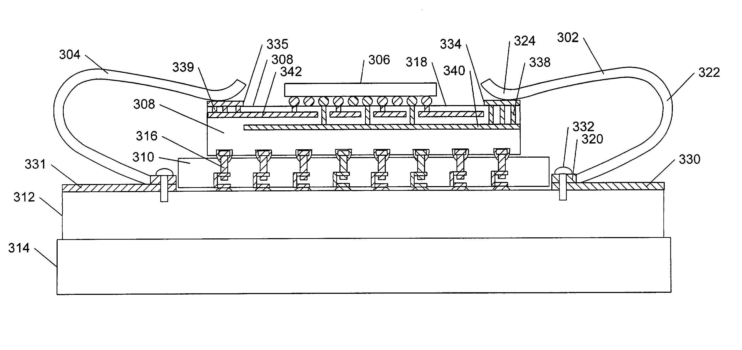
[0027]Various embodiments of the present invention provide a clamp, which attaches to a substrate and contacts a portion of the top surface of a housing. In one embodiment, the clamp includes a contact plate, which attaches to the substrate, a spring arm, which extends in an upward direction from the substrate, and a contact flange, which compresses against the to...
PUM
| Property | Measurement | Unit |
|---|---|---|
| conductive | aaaaa | aaaaa |
| current | aaaaa | aaaaa |
| currents | aaaaa | aaaaa |
Abstract
Description
Claims
Application Information