Arrangement for connecting the terminal contacts of an electronic component to a printed circuit board and conductor support for such an arrangement

a technology of electronic components and terminal contacts, which is applied in the direction of printed circuit non-printed electric components, coupling device connections, instruments, etc., can solve the problems of particularly thin form and high risk of tearing, and achieve the effect of low for

Active Publication Date: 2005-12-20
II VI DELAWARE INC
View PDF5 Cites 15 Cited by
  • Summary
  • Abstract
  • Description
  • Claims
  • Application Information

AI Technical Summary

Benefits of technology

[0011]The present invention is based on the object of providing an arrangement for connecting the terminal contacts of an electronic component to a printed circuit board which is particularly space-saving and with which only low forces are exerted on existing soldered connections. Furthermore, it is intended to provide a conductor support for use in such an arrangement.
[0018]The solution according to the invention is extremely space-saving, since scarcely any additional space is required on the surface of the printed circuit board for the connection to the conductor support. The alignment of the conductor support perpendicular to the surface of the printed circuit board also achieves the effect that only one bend of the conductor support is required. As a result, the shear loading of the soldering of the conductor support on the printed circuit board is reduced, so that its durability is improved. Since the remaining bend is at a distance from the contact regions of the conductor support, tensile loading of the interconnects of the conductor support is also additionally reduced. This is of significance in particular for the radio-frequency interconnects, which are of a particularly thin form and are particularly at risk of tearing.
[0019]The solution according to the invention further allows a locational separation of the adhesive bonding and soldering of the conductor support on the printed circuit board, whereby reworking of the soldered and adhesively bonded connections is made easier. Consequently, the soldering points and adhesive-bonding points can be detached at different times. In one configuration it is also possible in an advantageous way to dispense entirely with an adhesive bond, since adequate mechanical strength of the connection is already provided by the soldering itself.
[0022]In a development of this configuration, it is provided that the first portion of the conductor support has two rows of first contact regions. The contact regions of the first row are connected to electrical contacts on the one surface of the printed circuit board and the contact regions of the second row are connected to electrical contacts on the other surface of the printed circuit board. This allows the required space on the printed circuit board to be kept small in spite of a high number of contacts.
[0024]It has already been noted that the conductor support is preferably bent only once between the first portion and the second portion of the conductor support, for instance by approximately 180°. This has the effect of reducing shearing stresses and tensile stresses that occur.
[0031]The conductor support according to the invention consequently has a reduced width in the third portion, which is bent when the conductor support is used. As a result, a bending portion of the conductor support is defined and established, since the conductor support can be bent most easily in the portion of reduced width. The ease of handling the conductor support is improved in this way. The space requirement of the conductor support is also reduced by the provision of a portion of reduced width.

Problems solved by technology

This is of significance in particular for the radio-frequency interconnects, which are of a particularly thin form and are particularly at risk of tearing.

Method used


Image

  • Arrangement for connecting the terminal contacts of an electronic component to a printed circuit board and conductor support for such an arrangement
  • Arrangement for connecting the terminal contacts of an electronic component to a printed circuit board and conductor support for such an arrangement
  • Arrangement for connecting the terminal contacts of an electronic component to a printed circuit board and conductor support for such an arrangement

Examples


Embodiment Construction

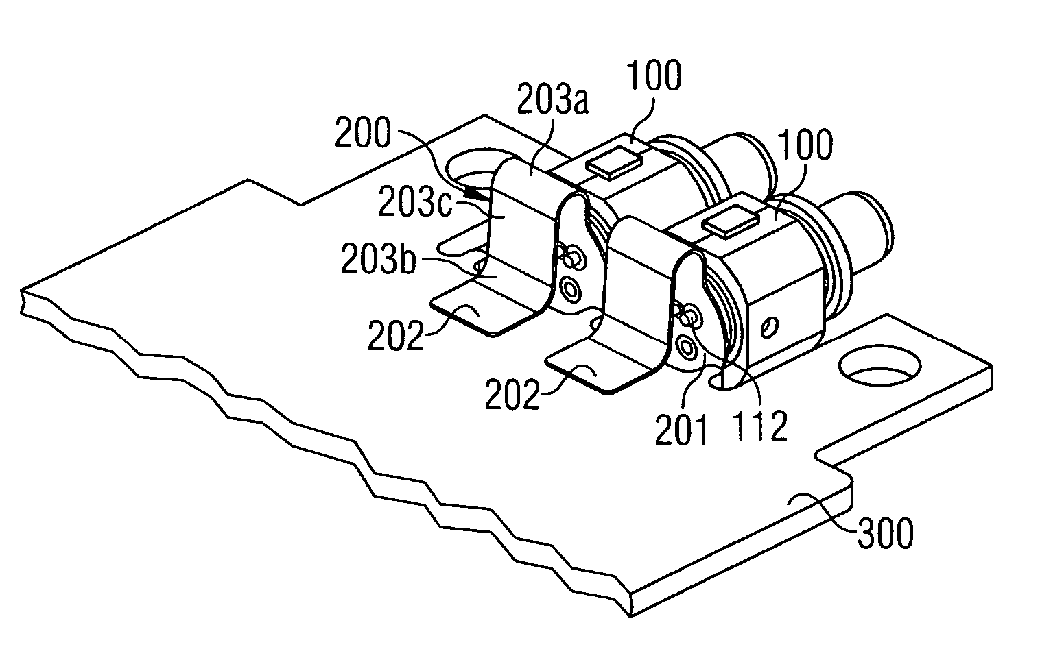
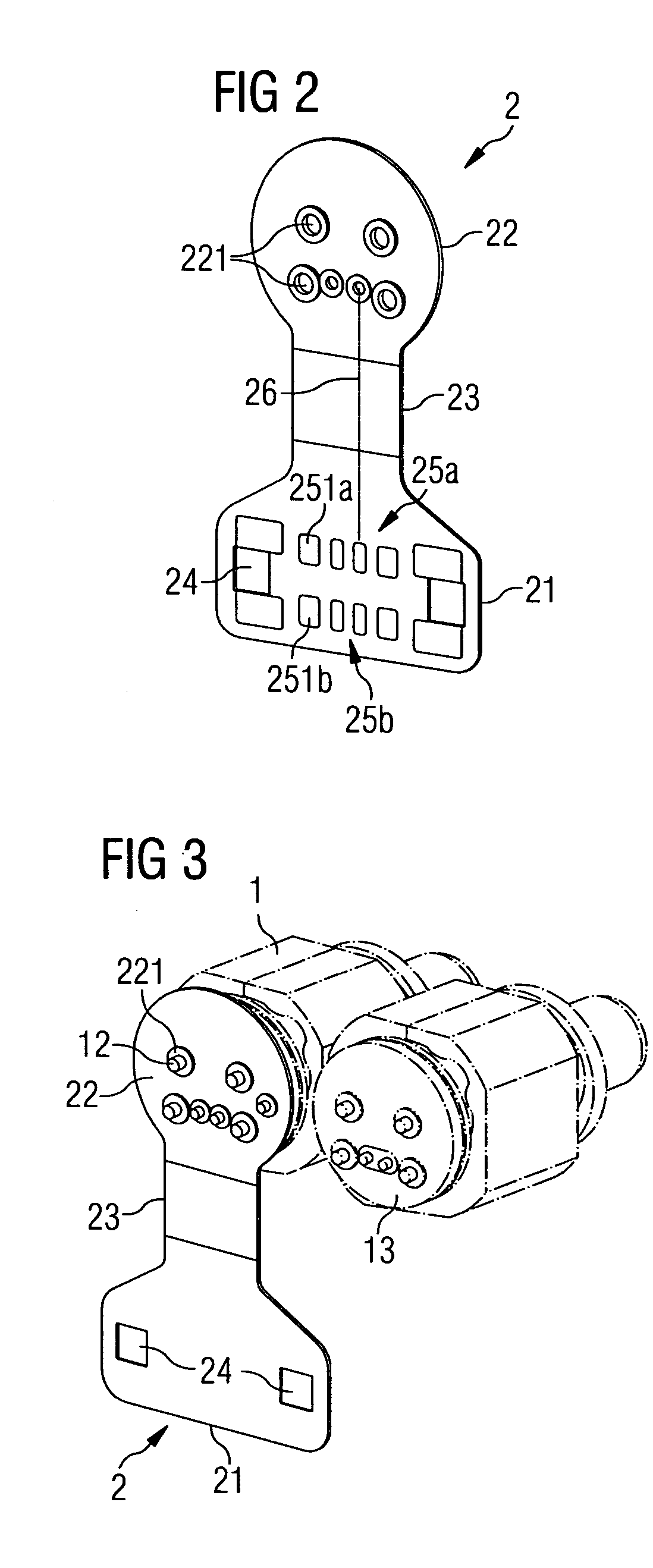
[0043]FIG. 1 shows an arrangement for connecting the terminal contacts of an electronic component to a printed circuit board which has two electronic components 1, respectively assigned flexible conductors 2 and a printed circuit board 3.

[0044]In the exemplary embodiment represented, the electronic components 1 are optoelectronic components, which convert electrical signals into optical signals, or vice versa. One of the two optoelectronic components 1 arranged next to each other is in this case preferably a transmitting component and the other is a receiving component. For optical coupling to an optical fiber, a plug region 11 is provided. However, it is pointed out that the arrangement is suitable in principle for the contacting of any desired electronic components.

[0045]For their contacting, the optoelectronic components 1 have electrical contacts 12, which are illustrated well in FIG. 3. In the exemplary embodiment represented, they are terminal pins 12, which protrude from a ba...


PUM


Abstract

An arrangement for connecting the terminal contacts of an electronic component to electrical contacts formed on a printed circuit board. An at least partly flexible conductor support having a plurality of interconnects provides an electrical connection between the terminal contacts of the electronic component and the electrical contacts of the printed circuit board such that a portion of the conductor support that is connected to the printed circuit board is arranged on an end face of the printed circuit board and extends perpendicularly in relation to the upper and lower surfaces of the printed circuit board. Furthermore, a conductor support formed with relatively narrow middle portion is provided to facilitate such an arrangement.

Description

RELATED APPLICATION[0001]The present application claims priority of U.S. patent application Ser. No. 60 / 512,028 filed by Andreas Stockhaus and Christian Carstens on Oct. 17, 2003.FIELD OF THE INVENTION[0002]The invention relates to an arrangement for connecting the terminal contacts of an electronic component to a printed circuit board and to a conductor support for such an arrangement. In particular, the invention relates to the electrical connection of the terminal pins of an optical transmitting and / or receiving device to a printed circuit board using a flexible conductor.BACKGROUND OF THE INVENTION[0003]It is known from DE 100 64 577 A1 to solder the terminal pins of a TO package which contains an optical transmitting and / or receiving device directly to a printed circuit board. Since both the printed circuit board and the TO package are fixed in a common housing (usually a transceiver housing), inadmissibly high mechanical stresses can occur, however, at the soldering points due...

Claims


Application Information

Patent Timeline
Patent Type & Authority Patents(United States)
IPC IPC(8): G02B6/38H01R12/00H01R12/71H05K1/14H05K1/18
CPCG02B6/3897H05K1/147H05K1/189H05K2201/049H05K2201/10121H05K2201/10446
Inventor STOCKHAUS, ANDREASCARSTENS, CHRISTIAN
Owner II VI DELAWARE INC
Why Eureka
Try Eureka