Semiconductor device including high speed transistors and high voltage transistors disposed on a single substrate

Inactive Publication Date: 2005-12-20
SONY CORP
View PDF17 Cites 18 Cited by
  • Summary
  • Abstract
  • Description
  • Claims
  • Application Information

AI Technical Summary

Benefits of technology

[0038]Furthermore, since the operating speeds and the voltages are changed by changing the impurity concentrations and the depths of the fir

Problems solved by technology

Consequently, it has been difficult to form a high speed bipolar tra

Method used


Image

  • Semiconductor device including high speed transistors and high voltage transistors disposed on a single substrate
  • Semiconductor device including high speed transistors and high voltage transistors disposed on a single substrate
  • Semiconductor device including high speed transistors and high voltage transistors disposed on a single substrate

Examples


Example

[0059]Preferred embodiments of the invention will now be described in detail with reference to the accompanying drawings.

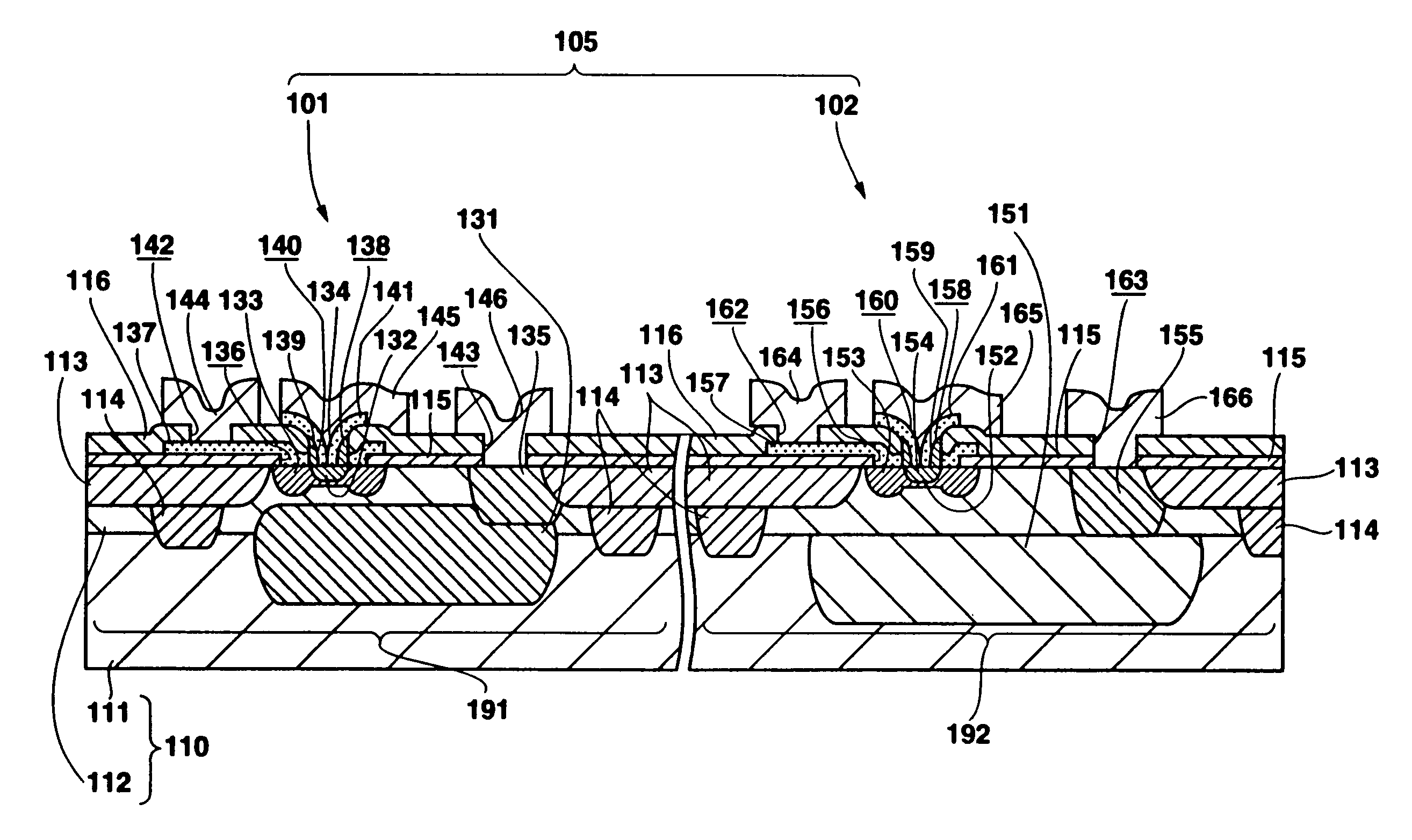
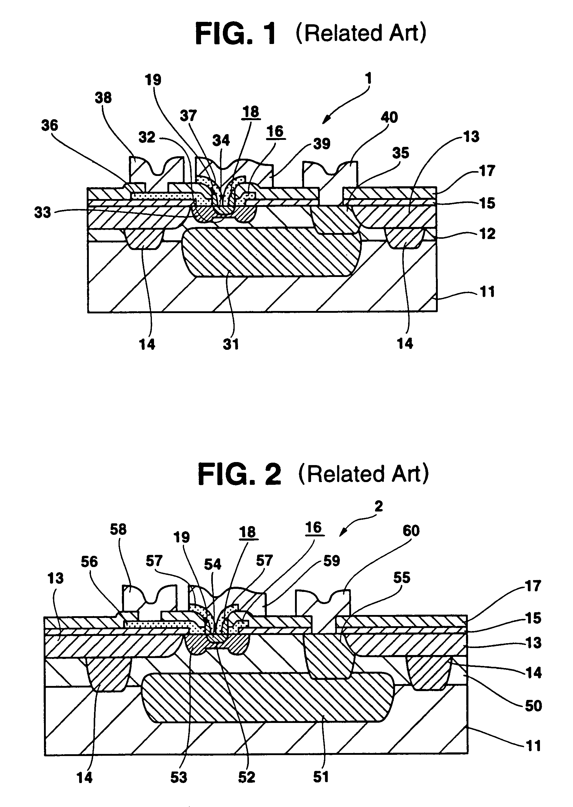
[0060]A semiconductor device of a first preferred embodiment of the invention will be described with reference to the schematic sectional construction view of FIG. 5. In FIG. 5, as an example, a high speed NPN bipolar transistor (hereinafter referred to as the first bipolar transistor) and a high voltage NPN bipolar transistor (hereinafter referred to as the second bipolar transistor) forming a so-called double silicon structure and having self-aligningly formed emitters and bases are shown.

[0061]As shown in FIG. 5, an N-type epitaxial layer 112 is formed on a P-type silicon substrate 111.

[0062]A device separating oxide film 113 for separating a first bipolar transistor formation region 191 and a second bipolar transistor formation region 192 is formed in the N-type epitaxial layer 112. A P+-type device separating diffusion layer 114 reaching the silicon substrate...


PUM


Abstract

In a semiconductor device comprising a first bipolar transistor and a second bipolar transistor having different voltages formed on a semiconductor substrate made by forming an epitaxial layer on a silicon substrate, in an upper part of the silicon substrate the first bipolar transistor has an N+-type first embedded diffusion layer having an impurity concentration higher than that of the epitaxial layer and the second bipolar transistor has an N-type second embedded diffusion layer having a lower impurity concentration and a deeper diffusion layer depth than the first embedded diffusion layer, whereby a high speed bipolar transistor and a high voltage bipolar transistor are formed on the same substrate.

Description

RELATED APPLICATION DATA[0001]This patent is a divisional application of Ser. No. 08 / 762,779, filed on Dec. 10, 1996, and issued as U.S. Pat. No. 5,976,940. Moreover, this patent claims priority to Japanese Application No. P07-322962, filed Dec. 12, 1995, which application is incorporated by reference to the extent permitted by law.BACKGROUND OF THE INVENTION[0002]1. Field of the Invention[0003]This invention relates to a semiconductor device wherein a high speed vertical type bipolar transistor and high voltage vertical type bipolar transistor are formed on the same substrate and a method of making the same.[0004]2. Description of the Related Art[0005]A vertical type NPN bipolar transistor of the related art constructed as a high speed bipolar transistor and a vertical type NPN bipolar transistor of the related art constructed as a high voltage bipolar transistor will be described with reference to FIG. 1 and FIG. 2.[0006]FIG. 1 is a schematic sectional view of the construction of ...

Claims


Application Information

Patent Timeline
IPC IPC(8): H01L29/73H01L21/331H01L21/8222H01L27/06H01L29/732
CPCH01L21/8222H01L29/70
Inventor GOMI, TAKAYUKIAMMO, HIROAKI
Owner SONY CORP
Why Eureka
Try Eureka