Alignment treatment of liquid crystal display device

a liquid crystal display and alignment treatment technology, applied in the manufacture of electrode systems, electric discharge tubes/lamps, instruments, etc., can solve the problems of polarized ultraviolet rays, inconvenient practical use, and the loss of thin film transistors in the active matrix

Inactive Publication Date: 2008-12-18
SHARP KK
View PDF23 Cites 5 Cited by
  • Summary
  • Abstract
  • Description
  • Claims
  • Application Information

AI Technical Summary

Benefits of technology

[0017]It is an object of the present invention to provide a liquid crystal display device which prevents the occurrence of a state where an electric charge remains in large amounts near one of the opposing alignment layers and the image previously displayed remains slightly sticked, due to the residual electric charge, even after the voltage is no longer applied.
[0018]Another object of the present invention is to provide a liquid crystal display device, having divided alignments, which enables the opposing alignment layers to be simultaneously oriented with ease.
[0047]According to this constitution, it is possible to realize the alignment of the liquid crystal by the irradiation of the ultraviolet rays, which is the easier means, and without using the rubbing (therefore, without the formation of pit-like rubbing traces which may be caused in the surface of the alignment layers by rubbing), and it is also possible to form a plurality of regions having different threshold voltages. Accordingly, it is possible to improve the viewing angle characteristic without increase in a production cost.
[0049]According to this constitution, it is possible to prevent any occurrence of extremely bright portions at the crosswise boundary line dividing four regions.

Problems solved by technology

There exists a further problem in rubbing.
Besides, the rubbing generates static electricity which may destroy TFTs (thin-film transistors) in the active matrix.
With this method, however, a problem exists in that polarized ultraviolet rays must be used.
However, the Glen-Taylor type polarizer is obtained by cutting a natural calcite and is not suited for practical use.
Therefore, a difference develops in the alignment treatment between the opposing portions of the two alignment layers, and the electric charge tends to remain in large amounts near one of the alignment layers.

Method used


Image

  • Alignment treatment of liquid crystal display device
  • Alignment treatment of liquid crystal display device
  • Alignment treatment of liquid crystal display device

Examples


first embodiment

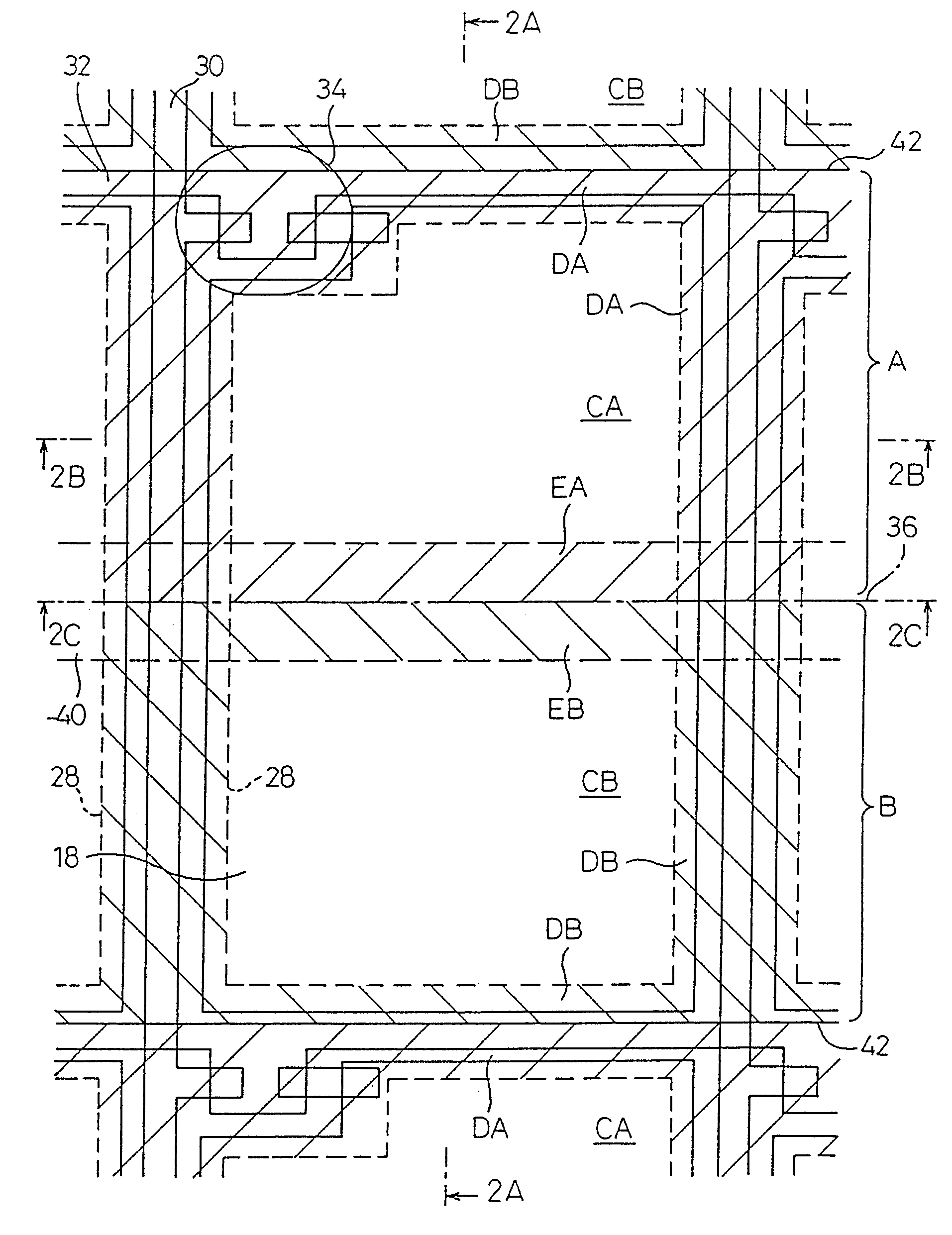
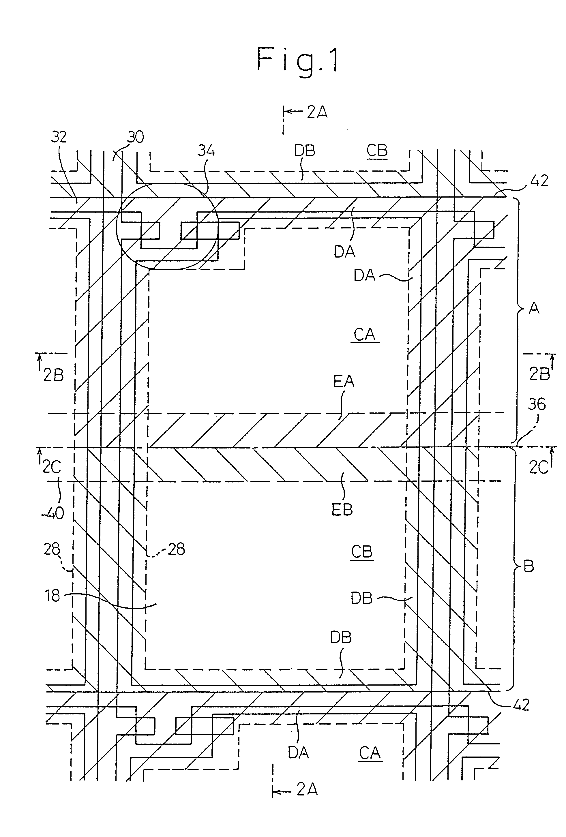
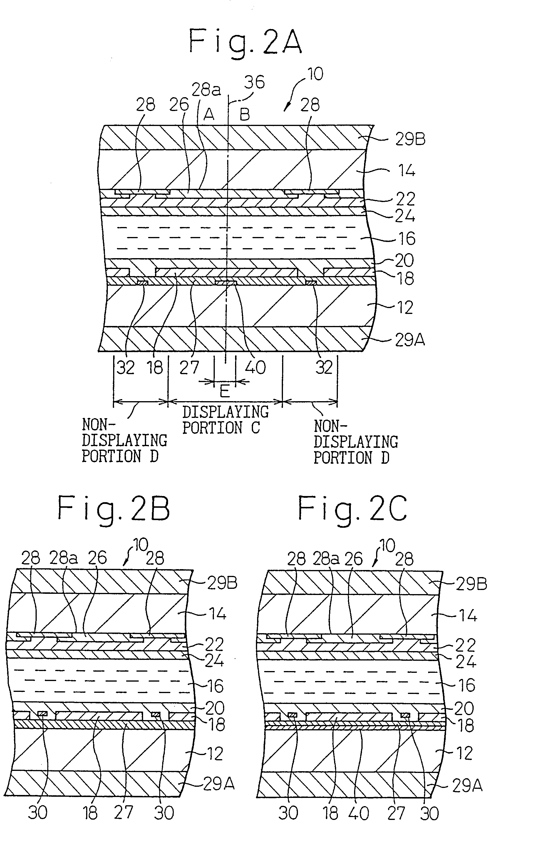
[0120]FIG. 1 is a plan view schematically illustrating a portion of a liquid crystal display device according to the present invention, FIGS. 2A to 2C are cross-sectional views illustrating the liquid crystal display device of FIG. 1, and FIG. 3 is a view illustrating an active matrix formed on one substrate of FIG. 2. In particular, FIG. 2A is a cross-sectional view taken along the line 2A-2A in FIG. 1, FIG. 2B is a cross-sectional view taken along the line 2B-2B in FIG. 1, and FIG. 2C is a cross-sectional view taken along the line 2C-2C in FIG. 1.

[0121]In FIGS. 2A to 2C, a liquid crystal display device 10 is constituted by a pair of spaced and opposed transparent glass substrates 12 and 14, and a liquid crystal layer 16 held between these substrates 12 and 14. On one substrate (lower substrate) 12 are formed transparent pixel electrodes 18 and a transparent alignment layer 20, and on the other substrate (upper substrate) 14 are formed a transparent common electrode 22 and a transp...

second embodiment

[0155]FIG. 16 is a view illustrating the present invention. Like the embodiment of FIG. 2, the liquid crystal display device 10 comprises a pair of spaced and opposed transparent glass substrates 12 and 14 and a liquid crystal layer 16 held between these substrates 12 and 14. On one substrate 12 are formed transparent pixel electrodes 18 and a transparent alignment layer 20, and on the other substrate 14 are formed a transparent common electrode 22 and a transparent alignment layer 24. On the upper substrate 14 are further formed a color filter 26 and a black matrix 28. The color filters 26 include color elements R, G and B. There is further provided a storage capacity electrode 40. The alignment layers realize alignments with pretilt angles, which are established without rubbing.

[0156]FIG. 17 illustrates an apparatus 60 for alignment-treating the alignment layer 20(24). The apparatus 60 for alignment treatment includes a source of light 62 for irradiating non-polarized ultraviolet ...

third embodiment

[0171]FIGS. 26A to 26D are views illustrating the alignment treatment according to the present invention. The alignment layer 20(24) shown here can be used in the liquid crystal display device shown in FIG. 16. Referring to FIG. 26A, the whole surface of the alignment layer 20 is rubbed with a rubbing roll 50, so that the liquid crystal molecules 16A are pretilted in a predetermined manner as shown in FIG. 26B. Referring to FIG. 26C, non-polarized ultraviolet rays 68A, 68B are projected in the opposite directions. Then, as shown in FIG. 26D, the realized pretilt angles in the domains A and B are the sums of a pretilt angle due to rubbing and pretilt angles due to irradiation with ultraviolet rays. Accordingly, a difference exists between the pretilt angles of the liquid crystal molecules in the two domains A and B.

[0172]The ultraviolet rays are irradiated in the manner described above. A lamp of the short arc-type is used as a source of light, ultraviolet rays of shorter than 280 nm...


PUM

PropertyMeasurementUnit
pretilt angleaaaaaaaaaa

Abstract

The liquid crystal display device comprising a pair of substrates with alignment layers formed thereon, and a liquid crystal filled between the substrates. Each pixel has pixel display portions CA, CB and non-display portions DA, EA, DB, EB. The pixel display portions are treated for realizing alignment in a different manner from the non-display portions and the alignment of the pixel display portions is controlled by the alignment of the non-display portions. Moreover, the alignment treatment is executed by the irradiation with ultraviolet rays in an inclined direction.

Description

[0001]This is a divisional of application Ser. No. 11 / 528,817, filed Sep. 28, 2006, which is a divisional of application Ser. No. 10 / 871,449, filed Jun. 14, 2004, now U.S. Pat. No. 7,133,099, which is a divisional of application Ser. No. 10 / 317,792, filed Dec. 12, 2002, now U.S. Pat. No. 6,781,656, which is a divisional of application Ser. No. 09 / 030,410, filed Feb. 25, 1998, now U.S. Pat. No. 6,512,564.BACKGROUND OF THE INVENTION[0002]1. Field of the Invention[0003]The present invention relates to a liquid crystal display device. More particularly, the present invention relates to a technology for alignment-treating the alignment layers of a liquid crystal display device.[0004]2. Description of the Related Art[0005]A liquid crystal display device includes a pair of spaced and opposed substrates, an electrode and an alignment layer formed on one substrate, an electrode and an alignment layer formed on the other substrate, and a liquid crystal held between the pair of substrates. The...

Claims


Application Information

Patent Timeline
Patent Type & Authority Applications(United States)
IPC IPC(8): G02F1/1337H01J9/00G02F1/1335G02F1/13
CPCG02F1/133512G02F1/133753G02F1/133784G02F1/133788G02F2001/133742G02F2001/133757G02F1/133742G02F1/133757G02F1/1337
Inventor YOSHIDA, HIDEFUMISEINO, TSUTOMUTASAKA, YASUTOSHI
Owner SHARP KK
Why Eureka
Try Eureka