Interconnect substrate and method of manufacture thereof, electronic component and method of manufacturing thereof, circuit board and electronic instrument

a technology of interconnect substrate and manufacturing method, which is applied in the direction of insulating substrate metal adhesion improvement, printed element electric connection formation, and association of printed circuit non-printed electric components, etc., and can solve the problem of not being able to reduce the cost to that of a conventional printed interconnect substra

Inactive Publication Date: 2005-12-20
SEIKO EPSON CORP
View PDF46 Cites 52 Cited by
  • Summary
  • Abstract
  • Description
  • Claims
  • Application Information

AI Technical Summary

Benefits of technology

[0005]The present invention solves this problem, and has as its object the provision of an inexpensive interconnect substrate and met

Problems solved by technology

However, a built-up interconnect substrate requires repeated steps of applying an interconnect and an insulating layer, and photosensitive resin

Method used


Image

  • Interconnect substrate and method of manufacture thereof, electronic component and method of manufacturing thereof, circuit board and electronic instrument
  • Interconnect substrate and method of manufacture thereof, electronic component and method of manufacturing thereof, circuit board and electronic instrument
  • Interconnect substrate and method of manufacture thereof, electronic component and method of manufacturing thereof, circuit board and electronic instrument

Examples


first embodiment

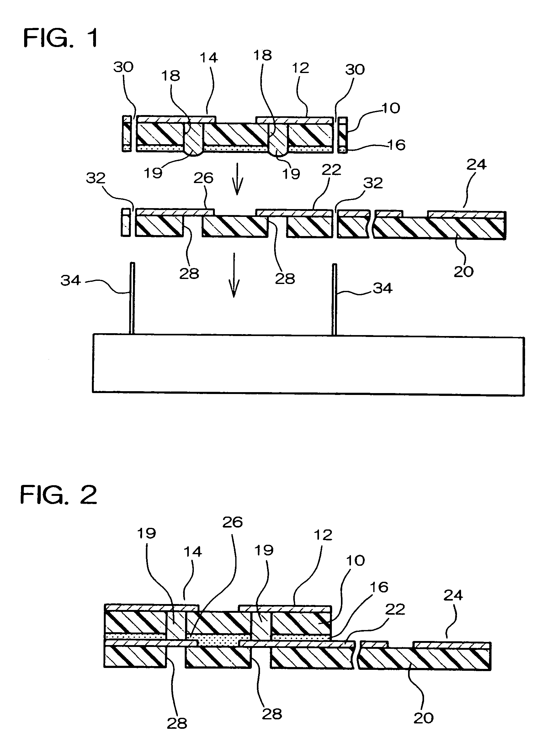
[0127]FIG. 1 illustrates the method of manufacture of the first embodiment of the interconnect substrate to which the present invention is applied, and FIG. 2 shows the first embodiment of the interconnect substrate to which the present invention is applied.

[0128]The interconnect substrate shown in FIG. 1 comprises a first substrate 10 and a second substrate 20, and can be used for example as an interposer of a semiconductor device.

[0129]The first and second substrates 10 and 20 may be formed of different materials, or may equally be formed of the same material. As the material may be used an organic material, or equally an inorganic material, or a composite of the two. As a first or second substrate 10 or 20 formed of an organic material may be used for example a flexible substrate formed of polyimide resin. As the flexible substrate may be used a tape used in FPC (Flexible Printed Circuit) or TAB (Tape Automated Bonding) technology. As the first or second substrate 10 or 20 formed...

second embodiment

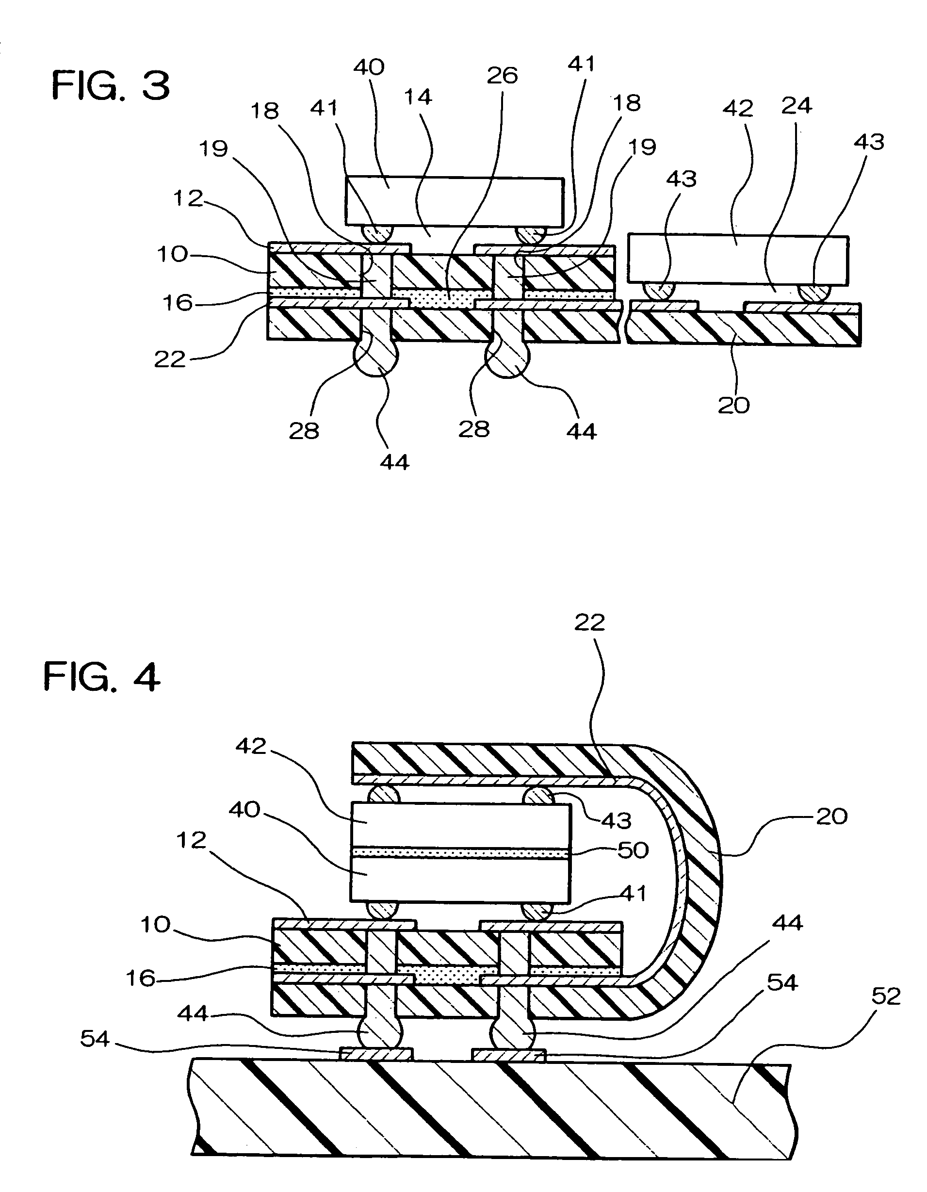
[0156]FIG. 3 shows a second embodiment of the semiconductor device to which the present invention is applied. This embodiment of the semiconductor device includes the interconnect substrate explained in the first embodiment. The interconnect substrate is as explained in the first embodiment, detailed description is omitted. The surface of the first substrate 10 opposite to that on which the first interconnect pattern 12 is formed is adhered to the surface of the second substrate 20 on which the second interconnect pattern 22 is formed.

[0157]In the mounting region 14 of the first substrate 10, the semiconductor chip 40 is mounted. The semiconductor chip 40 is electrically connected to the first interconnect pattern 12. In more detail, electrodes 41 of the semiconductor chip 40 are electrically connected to the first interconnect pattern 12. The electrodes 41 are commonly bonded to lands of the interconnect pattern 12. On at least either of the part of the interconnect pattern 12 conn...

third embodiment

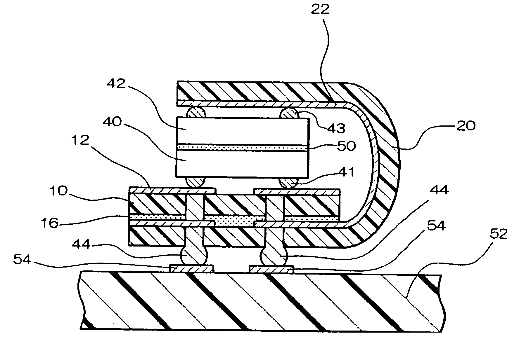
[0172]FIG. 4 shows a third embodiment of the semiconductor device to which the present invention is applied. This embodiment of the semiconductor device includes the structural elements of the semiconductor device described in the second embodiment, and as these structural elements are the same as described in the second embodiment, detailed description is omitted here. The surface of the first substrate 10 opposite to that on which the first interconnect pattern 12 is formed is adhered to the surface of the second substrate 20 on which the second interconnect pattern 22 is formed.

[0173]In this embodiment, the second substrate 20 is bent. The first semiconductor chip 40 and second semiconductor chip 42 are adhered. In more detail, the surface of the first semiconductor chip 40 opposite to the surface of mounting on the first substrate 10, and the surface of the second semiconductor chip 42 opposite to the surface of mounting on the second substrate 20 are adhered. For the adhesion, ...


PUM


Abstract

An interconnect substrate including a first substrate on which a first interconnect pattern is formed, having a mounting region for an electronic chip; and a second substrate on which a second interconnect pattern electrically connected to the first interconnect pattern is formed. The second substrate includes a region to which at least a part of the first substrate is adhered, and a mounting region for an electronic chip.

Description

[0001]This is a Division of application Ser. No. 09 / 807,601 filed Apr. 16, 2001, which in turn claims priority under 35 U.S.C. §365 of Japanese Patent Application No. 11-232565 filed Aug. 19, 1999 in Japan for National Stage of PCT / JP00 / 05395 on Sep. 11, 2000. The entire disclosures of the prior applications, together with the foreign priority application, are hereby incorporated by reference in their entirety.TECHNICAL FIELD[0002]The present invention relates to an interconnect substrate and method of manufacture thereof, to an electronic component and method of manufacture thereof, to a circuit board and to an electronic instrument.BACKGROUND ART[0003]In recent years the mounting density of electronic components has continued to rise, and very fine interconnect substrates are required. There is a limit to the degree to which the pattern of an interconnect substrate can be made finer when forming the interconnect pattern on one surface of the substrate only, and therefore built-up ...

Claims


Application Information

Patent Timeline
IPC IPC(8): H01L23/538H05K1/14H05K1/18H05K3/00H05K3/38H05K3/40H05K3/46
CPCH01L23/5385H01L23/5387H05K3/4084H05K3/4691H01L2224/16H01L2924/01078H01L2924/01079H01L2924/09701H05K1/141H05K1/189H05K3/386H05K3/4038H05K3/4614H05K3/4617H05K3/4652H05K2201/0195H05K2201/0305H05K2201/0394H05K2203/0195H01L2924/00014H01L2224/16227H01L2224/32145H01L2224/73253H01L2224/0401
Inventor HASHIMOTO, NOBUAKI
Owner SEIKO EPSON CORP
Why Eureka
Try Eureka