Mode transformation and loss reduction in silicon waveguide structures utilizing tapered transition regions

a transition region and waveguide technology, applied in the direction of optical waveguide light guide, instruments, optics, etc., can solve the problems of loss of rib or ridge waveguide formed in soi platform, etc., and achieve the effect of reducing the loss of optical mode mismatch between the silicon surface layer and the rib

Active Publication Date: 2005-12-27
CISCO TECH INC
View PDF2 Cites 34 Cited by
  • Summary
  • Abstract
  • Description
  • Claims
  • Application Information

AI Technical Summary

Benefits of technology

[0007]Mode mismatch between the silicon surface layer and the rib can be reduced in accordance with the present invention by using adiabatically-controlled tapers at the input...

Problems solved by technology

However, such rib or ridge waveguides formed in an SOI platform are known to suffer losses due to reflection, optical mode mismatch and unwanted Fabry-Perot resonances.
The optical mode mismatch loss is associated with the lack of perfect overlap of the optical mode between the silicon surface waveguiding struc...

Method used


Image

  • Mode transformation and loss reduction in silicon waveguide structures utilizing tapered transition regions
  • Mode transformation and loss reduction in silicon waveguide structures utilizing tapered transition regions
  • Mode transformation and loss reduction in silicon waveguide structures utilizing tapered transition regions

Examples


Embodiment Construction

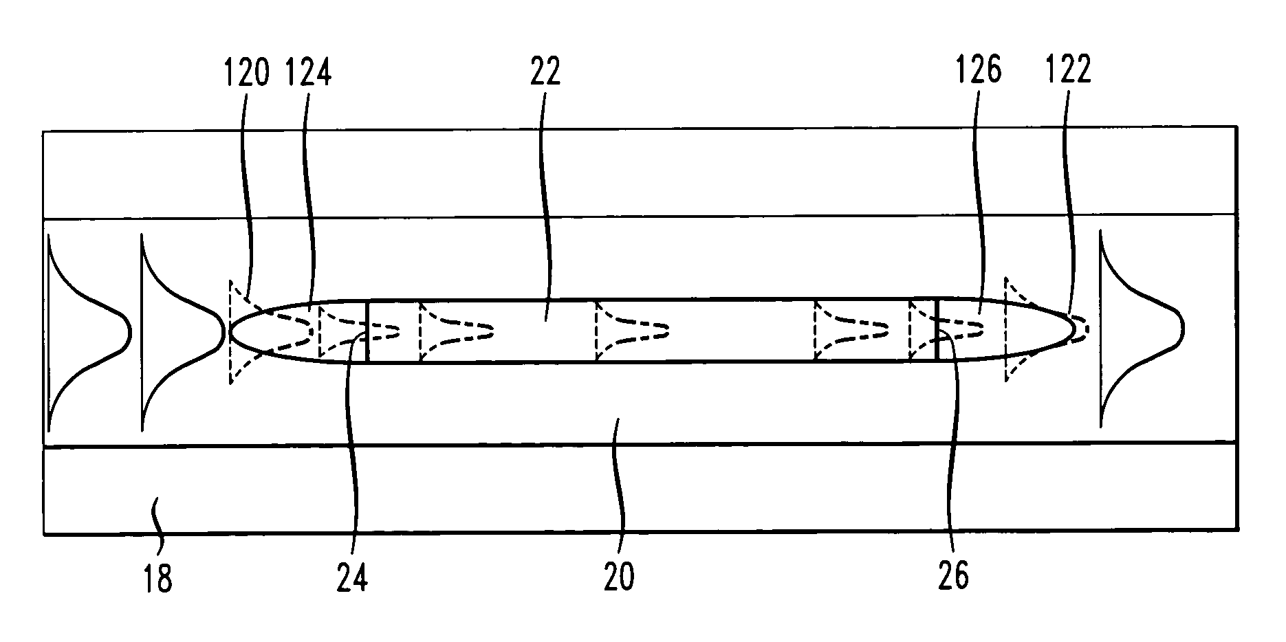
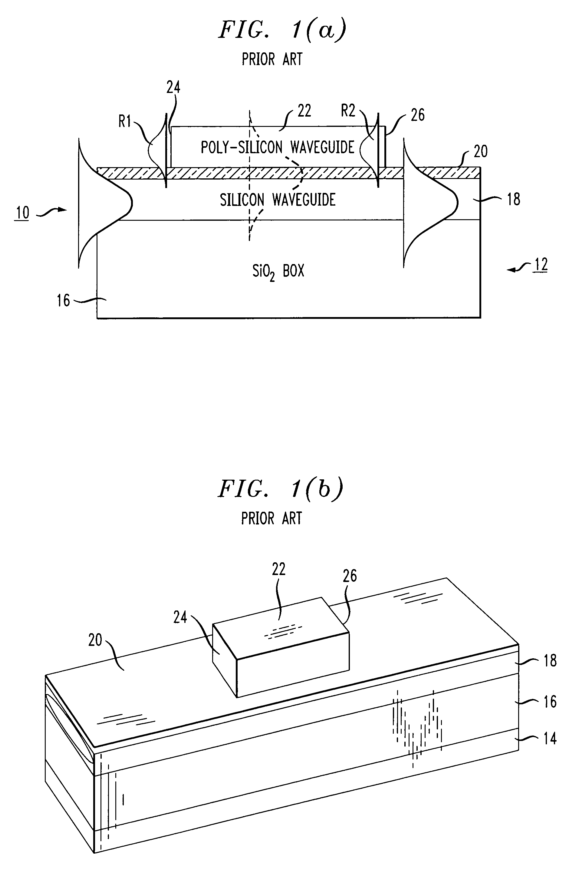
[0022]FIG. 1(a) contains a side view of an exemplary rib waveguide structure 10, this structure being described in detail in our co-pending application Ser. No. 10 / 146,321, filed May 15, 2002 now U.S. Pat. No. 6,898,352. For the purposes of the present invention, the configuration as shown in FIG. 1(a) particularly illustrates the presence of reflections at the input and output of the rib waveguide. An isometric view of the same rib waveguide structure 10 is illustrated in FIG. 1(b). As shown, structure 10 comprises an SOI platform 12 including a silicon substrate 14, a buried dielectric layer 16 and a relatively thin upper silicon layer 18. In this particular example, a relatively thin dielectric layer 20 is disposed across the top surface of upper silicon layer 18 and a rib waveguide structure 22 is formed along a portion of dielectric layer 20. The propagation of an exemplary optical signal is shown in FIG. 1(a), where the optical signal is first propagating within upper silicon ...


PUM


Abstract

A low loss coupling arrangement between a slab/strip waveguide and a rib waveguide in an optical waveguiding structure formed on a silicon-on-insulator (SOI) platform utilizes tapered sections at the input and/or output of the rib waveguide to reduce loss. Optical reflections are reduced by using silicon tapers (either vertical tapers, horizontal tapers, or two-dimensional tapers) that gradually transition the effective index seen by an optical signal propagating along the slab/strip waveguide and subsequently into and out of the rib waveguide. Loss can be further reduced by using adiabatically contoured silicon regions at the input and output of the rib waveguide to reduce mode mismatch between the slab/strip waveguide and rib waveguide. In a preferred embodiment, concatenated tapered and adiabatic sections can be used to provide for reduced optical reflection loss and reduced optical mode mismatch.

Description

CROSS REFERENCE TO RELATED APPLICATION[0001]This application claims the benefit of Provisional Application Ser. No. 60 / 462,050, filed Apr. 11, 2003.TECHNICAL FIELD[0002]The present invention relates to the utilization of silicon optical waveguide structures on a silicon-on-insulator (SOI) platform and, more particularly, to the utilization of tapered transition regions at the input and output of the silicon waveguide to provide for mode transformation and loss reduction in the optical system.BACKGROUND OF THE INVENTION[0003]Rib waveguides (also known as ridge waveguides) are known and used in optical transmission arrangements such as, for example, arrangements constructed upon and using silicon-on-insulator (SOI) devices. In an SOI arrangement, a rib waveguiding structure comprises a slab / strip waveguide region within the upper silicon layer of the SOI structure, with a silicon “rib” disposed along a portion of the surface of the upper silicon layer (there may or may not be a relati...

Claims


Application Information

Patent Timeline
IPC IPC(8): G02B6/12G02B6/122
CPCG02B6/1228G02B2006/12097
Inventor GOTHOSKAR, PRAKASHGHIRON, MARGARETPATEL, VIPULKUMARMONTGOMERY, ROBERT KEITHSHASTRI, KALPENDUPATHAK, SOHAMYANUSHEFSKI, KATHERINE A.
Owner CISCO TECH INC
Why Eureka
Try Eureka