

Single-crystalline film and process for production thereof
a single-crystalline film and film technology, applied in the field of single-crystalline films, can solve the problems of polycrystalline films and failure to provide single-crystalline films
- Summary
- Abstract
- Description
- Claims
- Application Information
AI Technical Summary
Benefits of technology
Problems solved by technology
Method used
Image

Examples
example 1
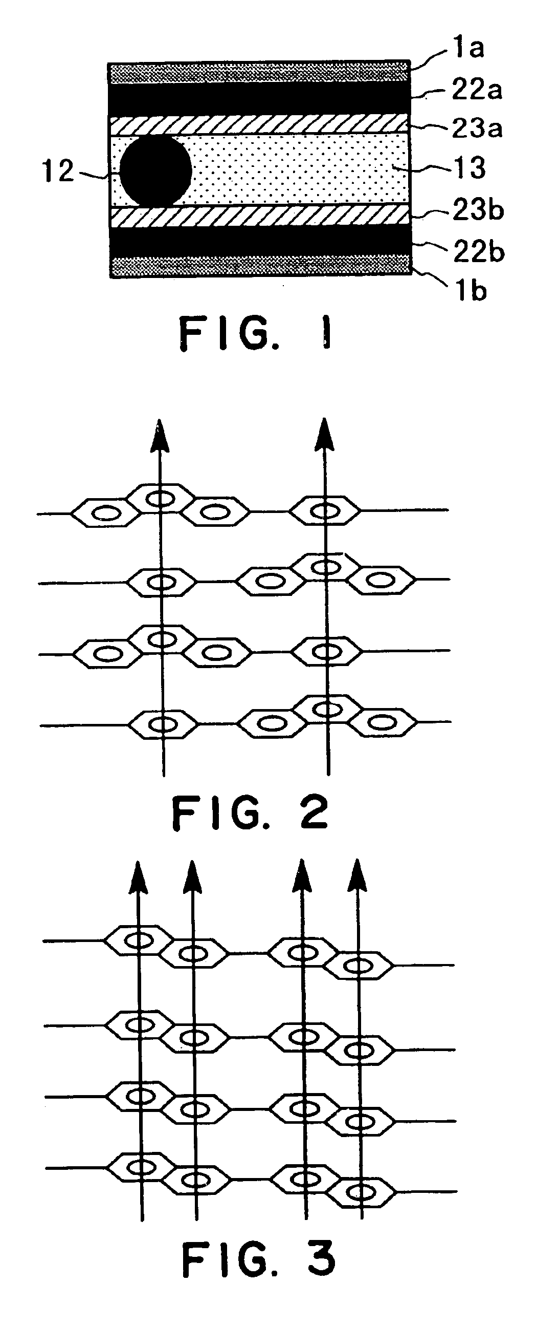
[0044]A cell having a layer structure schematically illustrated in FIG. 1 was prepared.
[0045]Two glass sheets each having a thickness of 1.1 mm and an areal size of ca. 20 mm×20 mm were respectively coated with a 700 Å-thick ITO transparent conductor film by sputtering and further with a 0.7 wt. % solution in NMP (N-methylpyrrolidone) of a polyamic acid (“LP-64”, made by Toray K. K.) having a recurring unit of formula (3) below by spin coating at 2000 rpm for 20 seconds:
followed by pre-drying at 80° C. for 5 minutes and baking at 200° C. for 60 minutes to form a 50 Å-thick film of polyimide represented by formula (4) below:
[0046]The polyimide film on each glass substrate was subjected four tines to rubbing in one direction with a nylon-planted cloth at a roller feed speed of 10 mm / sec and a roller revolution speed of 1000 rpm.
[0047]The two substrates treated in the above-described manner were applied to each other with 2.4 μ-diameter spacer beads disposed therebetween at a density...
example 1a
[0050]In order to examine the crystalline order of the respective regions in the crystalline film obtained in Example 1, a cell for x-ray diffraction analysis was prepared in the same manner as in Example 1 except 80 μm-thick glass substrates were used.
[0051]The cell was set in a rotary pair cathode-type x-ray diffraction apparatus (“RU-300”, made by Rigaku Denki K. K.) having an organization as illustrated in FIG. 10 to obtain x-ray diffraction patterns for the single crystal region (s-crystal) and polycrystal region (p-crystal), respectively, in FIG. 6 by a transmission method under the following conditions:[0052]X-ray source: CuKα, 40 kV, 200 mA[0053]Measurement conditions:[0054]Effective line focus width=0.05 mm[0055]S1=0.15 mm, S2=SS2 deg., S3=0.3 mm,[0056]Ni filter[0057]Focus-S1=95 mm, S1-Sample=90 mm,[0058]Sample-S2=143 mm, S2-S3=42 mm[0059]Incident angle (α deg.)=fixed[0060]2θ-scan 1 deg. / min., Interval=0.02 deg.[0061]Angle resolution=ca 3.5 rad (=ca. 0.2 deg.)[0062]Sample c...
example 2
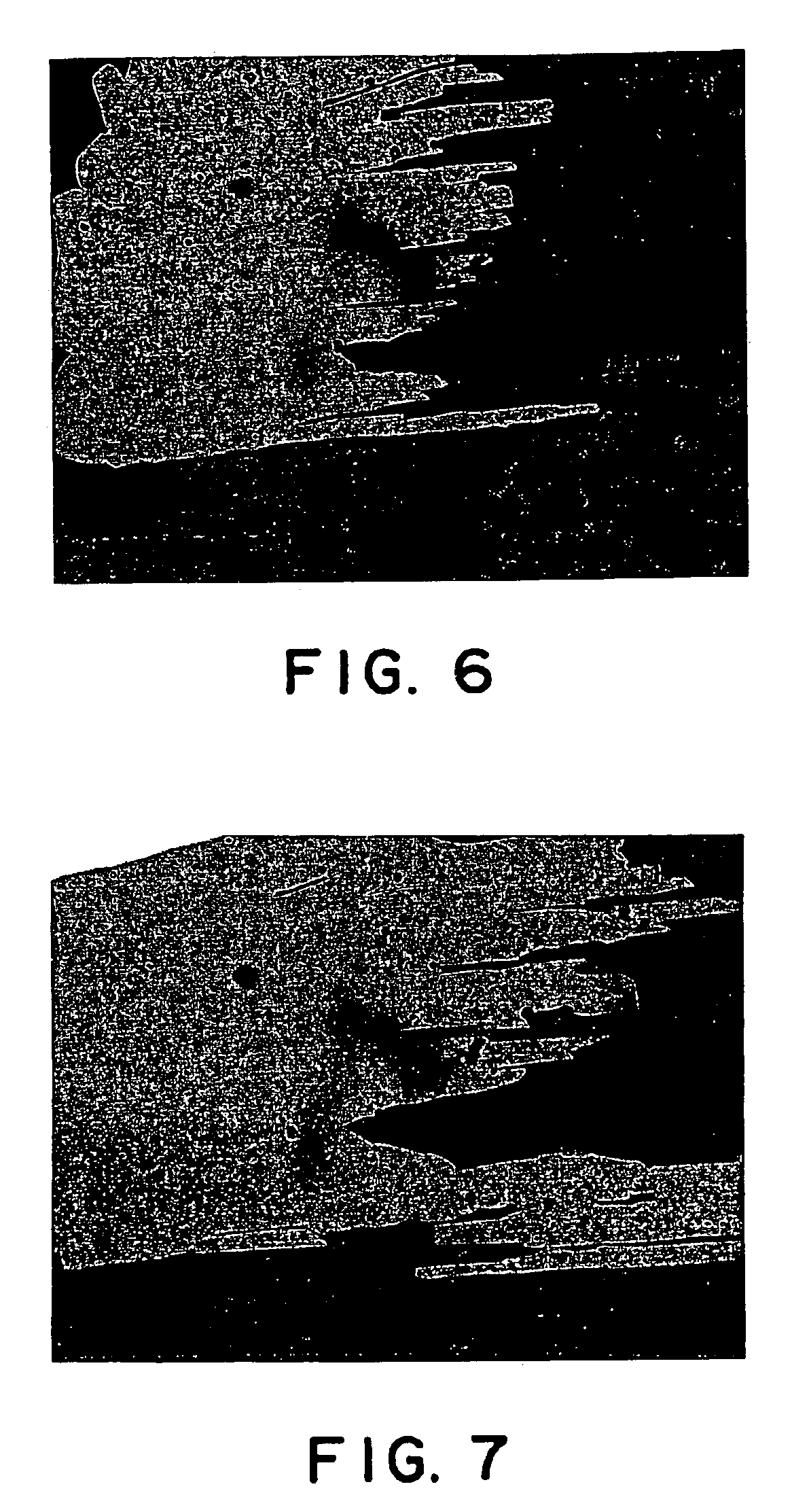
[0066]The cell prepared in Example 1 was again heated to a nematic phase temperature (130° C.) and thereafter started to be cooled at a rate of 1° C. / min, similar to Example 1. In this example, however, the cell was not continually cooled to room temperature as in Example 1, but held for 30 minutes at 118° C. which was a crystal phase temperature lower than the SmC-crystal transition temperature (=122° C.) and thereafter cooled to room temperature. In the meantime, the alignment states were photographed through a polarizing microscope after holding for 1 minute and 10 minutes, respectively, at 118° C. The thus-obtained photographs (each in a magnification of 100) are attached hereto as FIGS. 7 and 8, respectively.
[0067]With the lapse of time of the holding at 118° C., the single crystal region was remarkably enlarged to ca. 80% of the cell area (20 mm×20 mm) as shown in FIG. 7 after holding for 1 minute, which already exceeded the single crystal region percentage (ca. 50%) shown in ...
PUM
| Property | Measurement | Unit |
|---|---|---|
| thickness | aaaaa | aaaaa |
| thickness | aaaaa | aaaaa |
| transition temperature | aaaaa | aaaaa |
Abstract
Description
Claims
Application Information