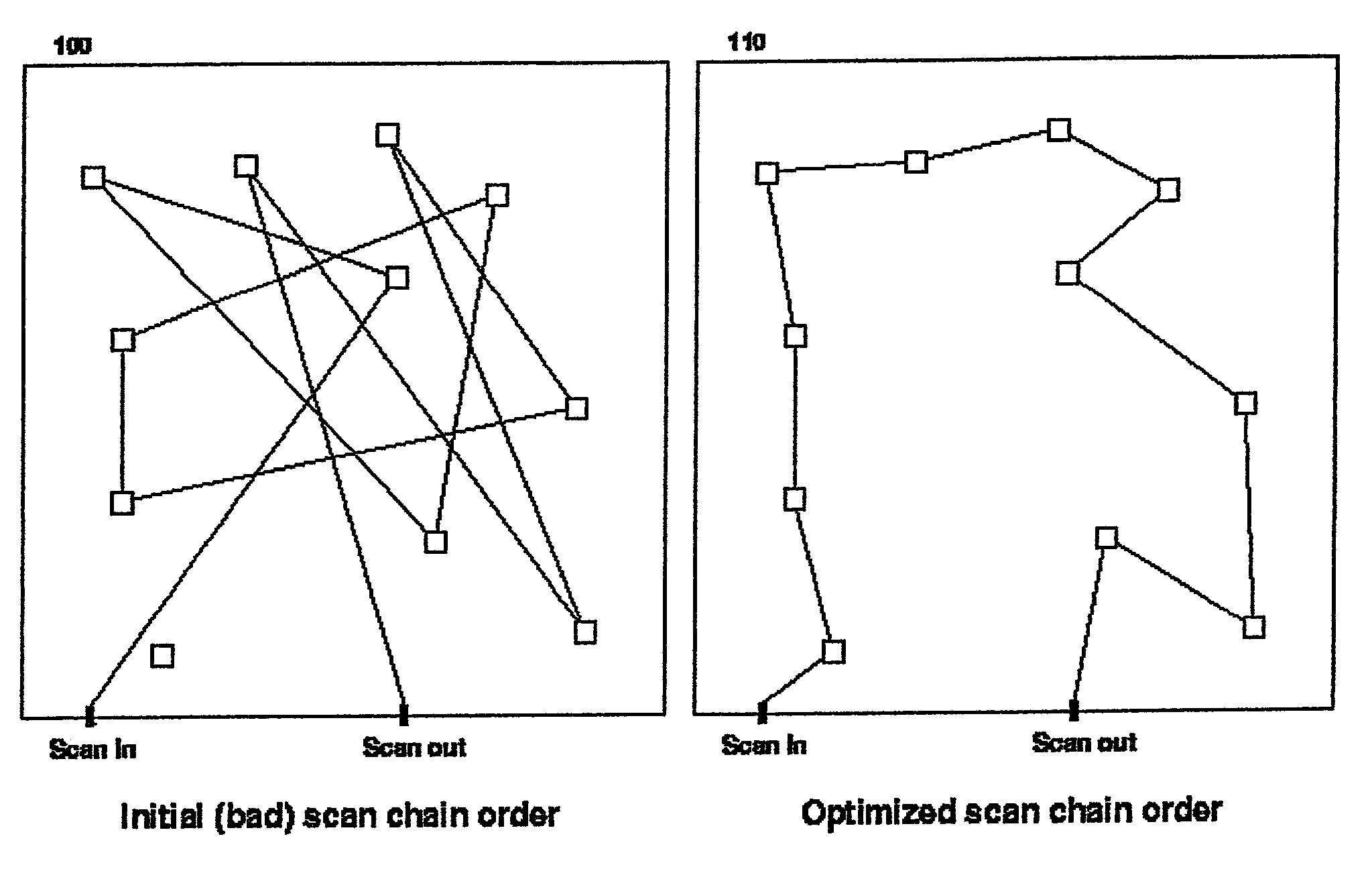
Method for reducing switching activity during a scan operation with limited impact on the test coverage of an integrated circuit
- Summary
- Abstract
- Description
- Claims
- Application Information
AI Technical Summary
Benefits of technology
Problems solved by technology
Method used
Image

Examples
Embodiment Construction
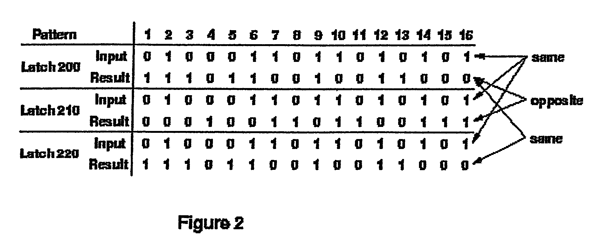
[0032]Considering a pair of memory elements to which certain stimulus values are applied and into which certain result values are stored for each set of precomputed test patterns, there are 16 possible combinations of stimulus and result values that can occur in any given test pattern, assuming that all stimulus and result values involved are specified (i.e., they are not don't care stimuli or undetermined results). If the pair of memory elements are connected adjacently in a scan chain, there will be a switching event propagated through the scan chain as the stimulus values for the two memory elements are scanned-in if they are to be loaded with opposite stimulus values with no intervening inversion between the two memory elements in the scan chain, or if they are to be loaded with the same stimulus values and there is an intervening inversion between the two memory elements in the scan chain. Similarly, there will be a switching event propagated through the scan chain as the resul...
PUM
 Abstract
Description
Claims
Application Information
 - R&D
- Intellectual Property
- Life Sciences
- Materials
- Tech Scout
- Unparalleled Data Quality
- Higher Quality Content
- 60% Fewer Hallucinations
Browse by: Latest US Patents, China's latest patents, Technical Efficacy Thesaurus, Application Domain, Technology Topic, Popular Technical Reports.
© 2025 PatSnap. All rights reserved.Legal|Privacy policy|Modern Slavery Act Transparency Statement|Sitemap|About US| Contact US: help@patsnap.com