High-voltage lateral transistor with a multi-layered extended drain structure

a drain structure and high-voltage transistor technology, applied in semiconductor devices, diodes, electrical devices, etc., can solve the problems of increasing on-state resistance, affecting the on-state performance of devices, and unable to meet the need for a high-voltage transistor structure that can support still higher voltages

Inactive Publication Date: 2006-01-17
POWER INTEGRATIONS INC
View PDF103 Cites 87 Cited by
  • Summary
  • Abstract
  • Description
  • Claims
  • Application Information

AI Technical Summary

Problems solved by technology

The combined decrease in doping and increase in the length of the extended drain region therefore have the deleterious effect on the on-state performance of the device, as both cause an increase in on-state resistance.
Although the device structures described above achieve high Vbd with relatively low on-state resistance as compared to earlier designs, there is still an unsatisfied need for a high-voltage transistor structure that can support still higher voltages while achieving a much lower on-state resistance.

Method used


Image

  • High-voltage lateral transistor with a multi-layered extended drain structure
  • High-voltage lateral transistor with a multi-layered extended drain structure
  • High-voltage lateral transistor with a multi-layered extended drain structure

Examples


Embodiment Construction

[0021]A high-voltage field-effect transistor having an extended drain and a method for making the same is described. The HVFET has a low specific on-state resistance and supports high voltage in the off-state. In the following description, numerous specific details are set forth, such as material types, doping levels, structural features, processing steps, etc., in order to provide a thorough understanding of the present invention. Practitioners having ordinary skill in the semiconductor arts will understand that the invention may be practiced without many of these details. In other instances, well-known elements, techniques, and processing steps have not been described in detail to avoid obscuring the invention.

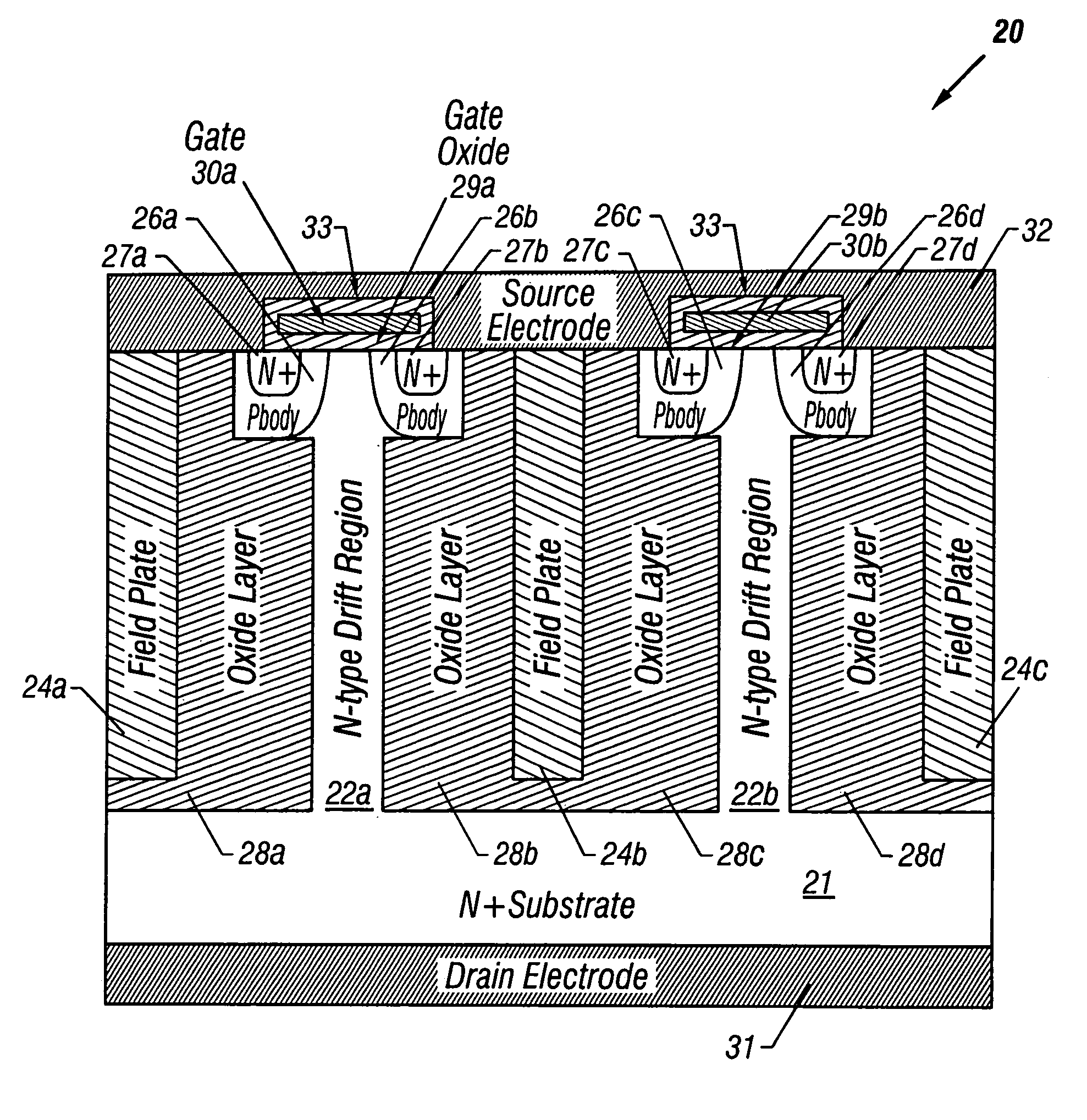
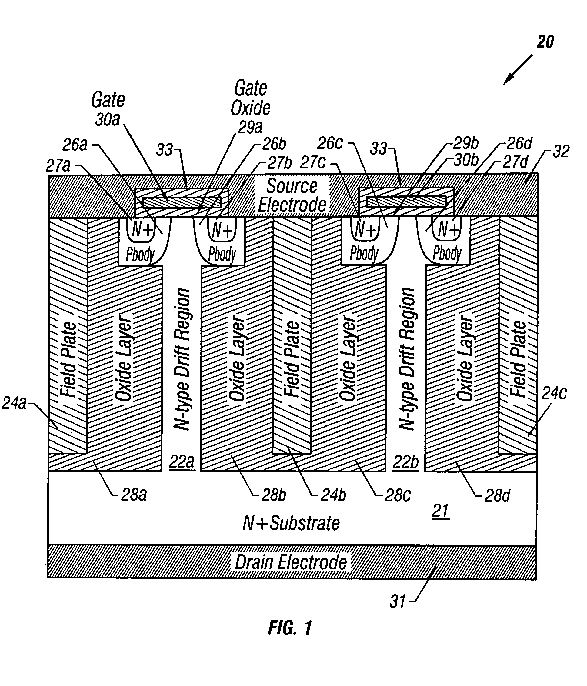
[0022]FIG. 1 is a cross-sectional side view of a vertical n-channel (i.e., NMOS) HVFET 20 in accordance with one embodiment of the present invention. It should be understood that the elements in the figures are representational, and are not drawn to scale in the interest of ...


PUM


Abstract

A high-voltage transistor with a low specific on-state resistance and that supports high voltage in the off-state includes one or more source regions disposed adjacent to a multi-layered extended drain structure which comprises extended drift regions separated from field plate members by one or more dielectric layers. The layered structure may be fabricated in a variety of orientations. A MOSFET structure may be incorporated into the device adjacent to the source region, or, alternatively, the MOSFET structure may be omitted to produce a high-voltage transistor structure having a stand-alone drift region. It is emphaized that this abstract is provided to comply with the rules requiring an abstract that will allow a searcher or other reader to quickly ascertain the subject matter of the technical disclosure. It is submitted with the understanding that it will not be used to interpret or limit the scope or meaning of the claims 37 CFR 1.72(b).

Description

RELATED APPLICATIONS[0001]This is a continuation application of Ser. No. 10 / 135,114, filed Apr. 30, 2002, now U.S. Pat. No. 6,815,293, which is a continuation-in-part application of application Ser. No. 09 / 948,422, filed Sep. 7, 2001, now U.S. Pat. No. 6,555,873, entitled, “HIGH-VOLTAGE LATERAL TRANSISTOR WITH A MULTI-LAYERED EXTENDED DRAIN STRUCTURE”, which applications are assigned to the assignee of the present application.FIELD OF THE INVENTION[0002]The present invention relates to semiconductor devices fabricated in a silicon substrate. More specifically, the present invention relates to field-effect semiconductor transistor structures capable of withstanding high voltages.BACKGROUND OF THE INVENTION[0003]High-voltage, field-effect transistors (HVFETs) are well known in the semiconductor arts. Most often, HVFETs comprise a device structure that includes an extended drain region that supports the applied high-voltage when the device is in the “off” state. HVFETs of this type are...

Claims


Application Information

Patent Timeline
Patent Type & Authority Patents(United States)
IPC IPC(8): H01L29/76H01L29/94H01L31/062H01L31/113H01L31/119H01L29/786H01L21/336H01L29/06H01L29/40H01L29/417H01L29/423H01L29/78H01L29/861
CPCH01L29/402H01L29/407H01L29/7802H01L29/7813H01L29/7824H01L29/7825H01L29/86H01L29/861H01L29/0653H01L2924/0002H01L29/41741H01L29/4232H01L29/42368H01L29/4238H01L2924/00H01L29/0886
Inventor DISNEY, DONALD RAYPAUL, AMIT
Owner POWER INTEGRATIONS INC
Why Eureka
Try Eureka