

Method for forming a multi-layered structure of a semiconductor device and methods for forming a capacitor and a gate insulation layer using the multi-layered structure
a multi-layered structure and semiconductor technology, applied in semiconductor devices, chemical vapor deposition coatings, coatings, etc., can solve the problems of serious reduction of low reduced so as to improve productivity and operation efficiency of deposition apparatus, the effect of rapid temperature change of semiconductor substra
- Summary
- Abstract
- Description
- Claims
- Application Information
AI Technical Summary
Benefits of technology
Problems solved by technology
Method used
Image

Examples
Embodiment Construction
[0030]Hereinafter, the embodiments of the present invention will be described in detail with reference to the accompanying drawings. In the drawings, like reference numerals identify similar or identical elements.
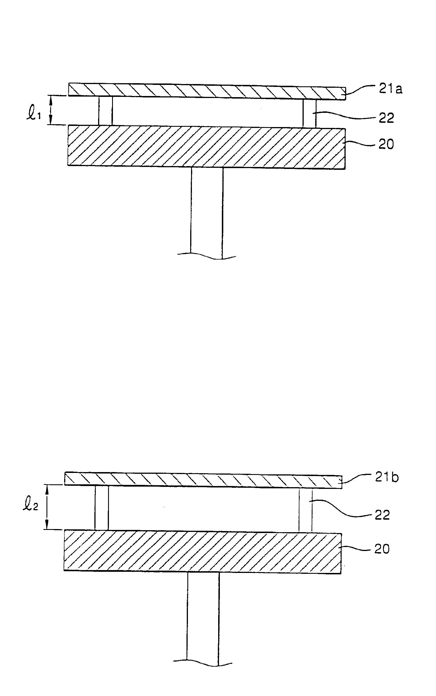
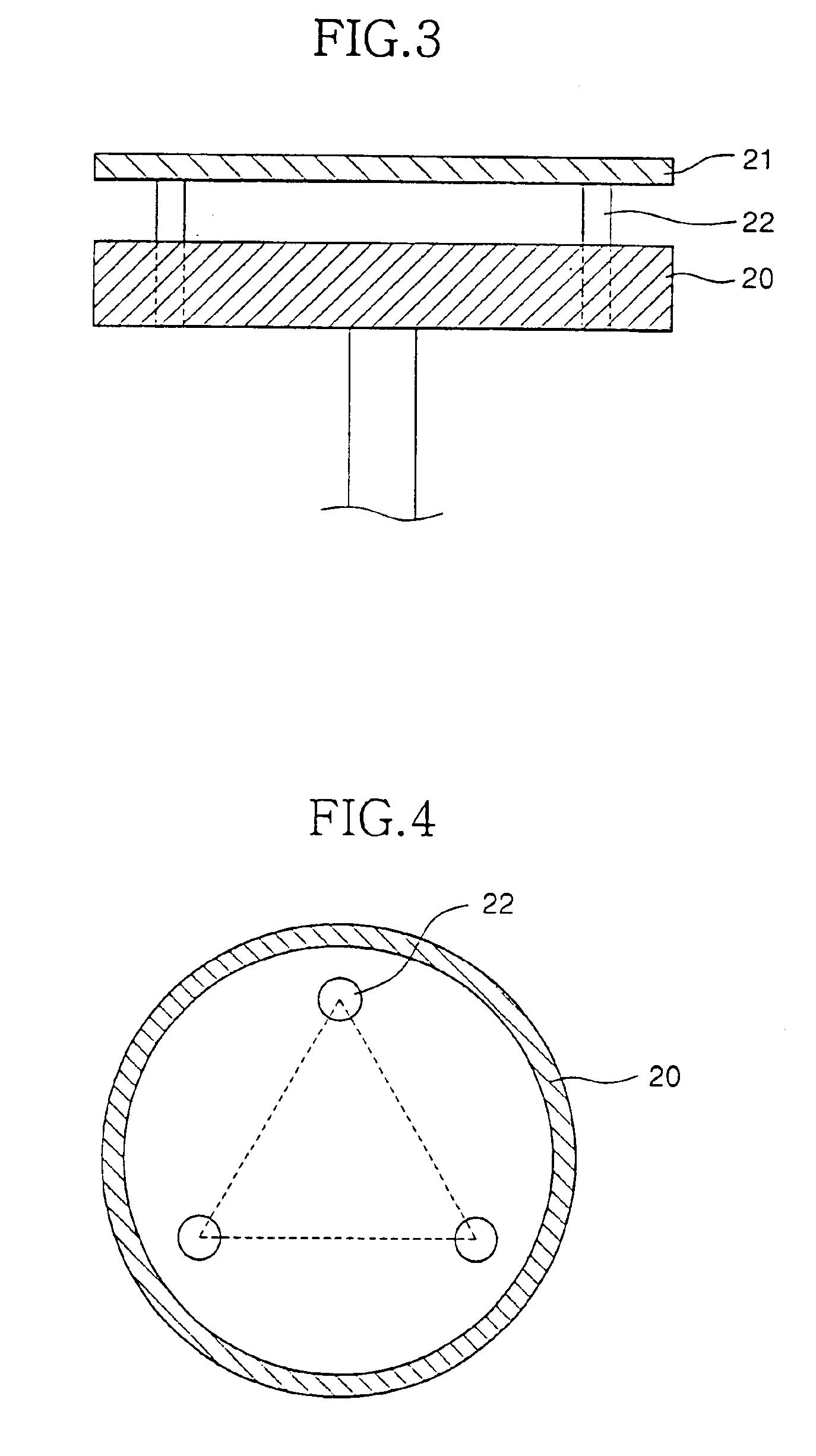
[0031]FIG. 3 is a schematic cross-sectional view illustrating the stage of a deposition apparatus for forming the multi-layered structure of a semiconductor device according to an embodiment of the present invention, and FIG. 4 is a plan view illustrating lift pins installed on the stage in FIG. 3.
[0032]Referring to FIG. 3, a stage 20 is provided to receive a semiconductor substrate 21 positioned thereon. The stage 20 is installed in the chamber of a deposition apparatus. The stage 20 can include a heater block for accelerating heat transfer to the substrate 21. When the semiconductor substrate 21 is positioned on the stage 20, the stage 20 provides the semiconductor substrate 21 with adequate heat to form thin films thereon through a heat transfer mechanism.
[0033]The stage...
PUM
| Property | Measurement | Unit |
|---|---|---|
| temperature | aaaaa | aaaaa |
| temperature | aaaaa | aaaaa |
| thermally conductive | aaaaa | aaaaa |
Abstract
Description
Claims
Application Information