Dual damascene process with no passing metal features

a damascene and metal feature technology, applied in the direction of semiconductor devices, semiconductor/solid-state device details, electrical apparatus, etc., can solve the problems of insufficient lateral expansion of the lateral expansion of the lateral expansion of the lateral expansion of the lateral expansion of the lateral expansion of the lateral expansion, and the difficulty in accurately positioning the via hole and the trench for the runners,

Inactive Publication Date: 2006-01-24
BELL SEMICON LLC +1
View PDF8 Cites 15 Cited by
  • Summary
  • Abstract
  • Description
  • Claims
  • Application Information

AI Technical Summary

Benefits of technology

[0009]Because the full via opening is etched before the formation of the trench, the photolithographic problems associated with the prior art methods are avoided. In fact, the design ...

Problems solved by technology

As the size of transistors has decreased, the size of other components has become a limiting factor in increasing overall component densities.
As the size of the openings decrease, accurate positioning of the holes for vias and the trenches for runners are more difficult to construct.
Thus, if the trench areas are exposed correctly in the photolithography process, the landing pad areas tend to be underexposed....

Method used


Image

  • Dual damascene process with no passing metal features
  • Dual damascene process with no passing metal features
  • Dual damascene process with no passing metal features

Examples


Embodiment Construction

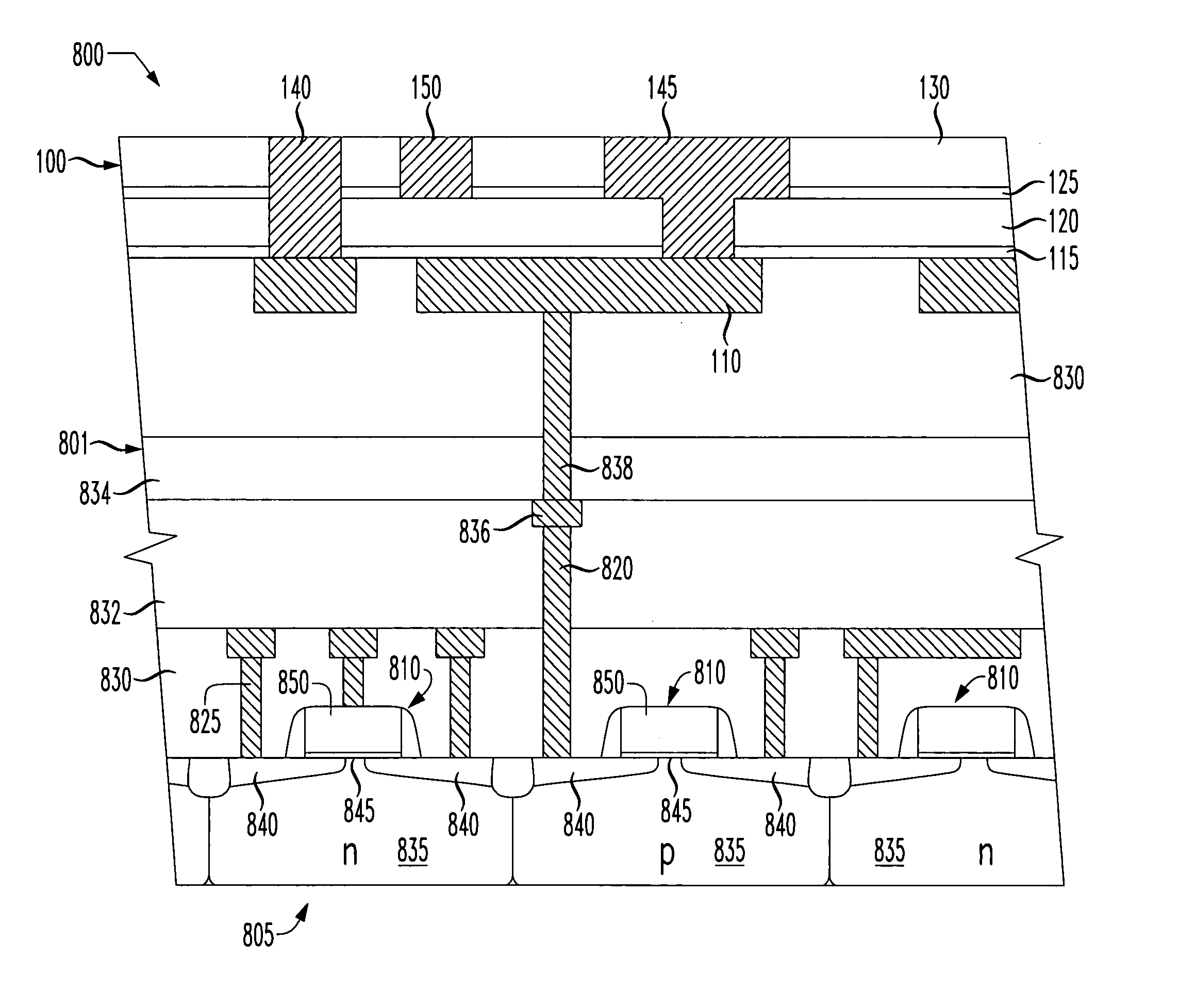
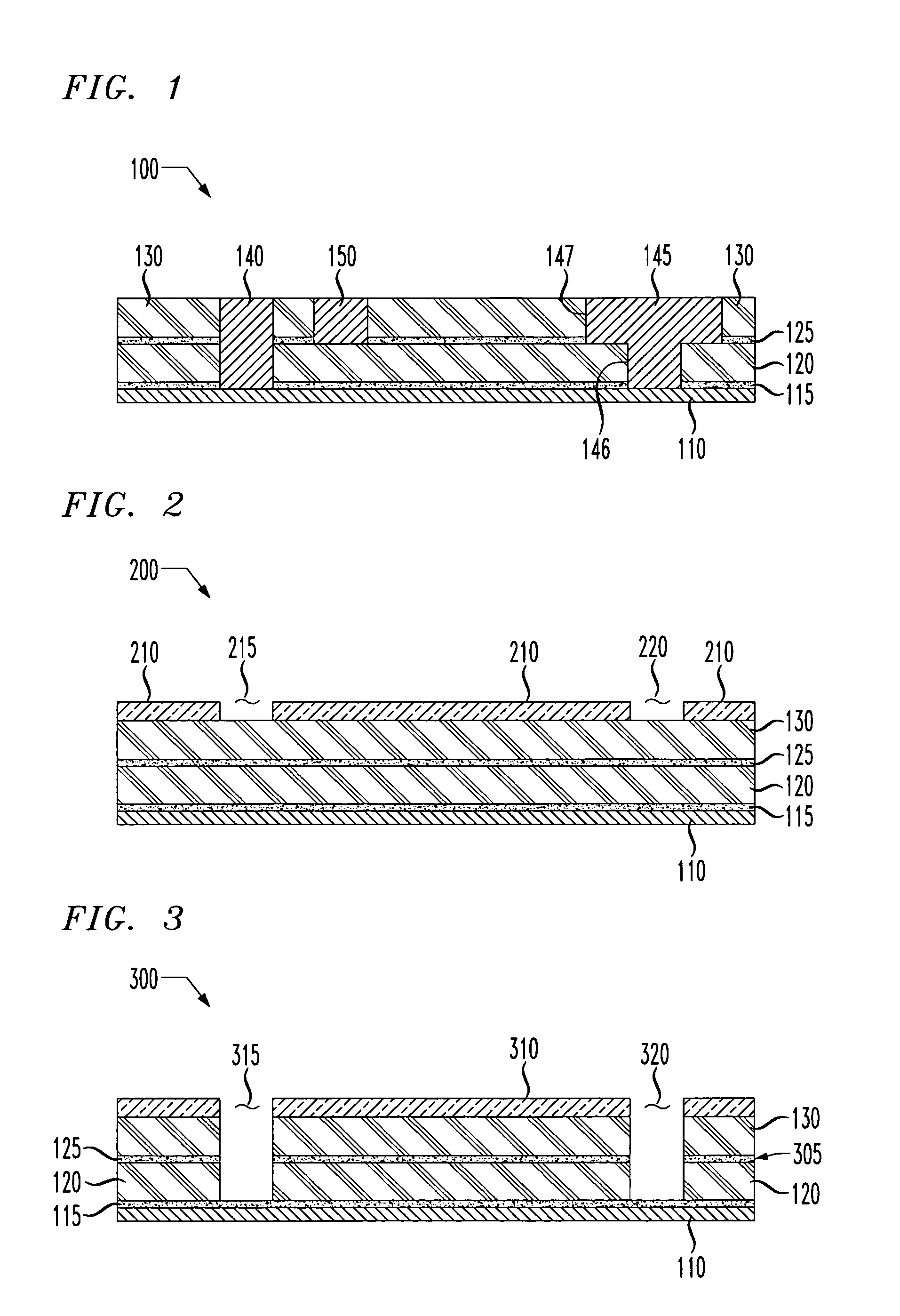
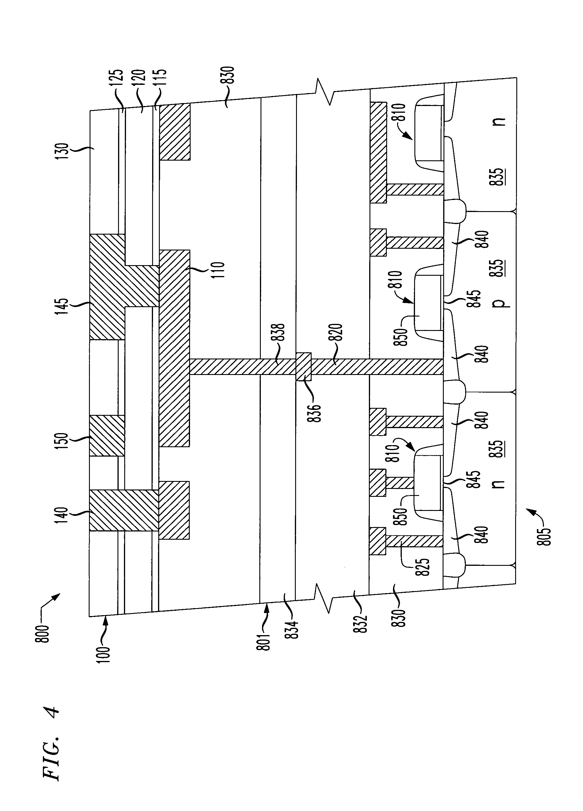
[0024]Referring initially to FIG. 1, illustrated is a partial sectional view of an exemplary embodiment of an interconnect structure 100 formed in accordance with the principals of the present invention. The interconnect structure 100 includes a first metal feature 110 located on a surface of a semiconductor device, first and second etch stop layers 115, 125, first and second dielectric layers 120, 130. The interconnect structure 100 also includes a first via 140 that has a first portion that extends from the conductive layer 110 to the second etch stop layer 125 and a second portion that extends from the second etch stop layer 125 through the second dielectric layer 130. It should be noted that the via 140 does not have a landing pad, which may also be known as a passing metal feature, associated with it. In many conventional devices the landing pad is a metal-filled trench that is located immediately over a via and serves as a connection point for an overlying via. In such convent...


PUM


Abstract

The present invention provides a method of forming integrated circuit interconnect structures wherein a passing metal feature does not include a landing pad. In an exemplary embodiment, the method includes forming a via opening through first and second dielectric layers, such as silicon dioxide layer, located over a conductive layer, such as copper, and to a first etch stop layer, such as silicon nitride, located over the conductive layer. A trench opening is then formed through the second dielectric layer and to a second etch stop layer. Once the via and trench openings are formed, an etch is conducted that etches through the first etch stop layer such that the opening contacts the underlying conductive layer.

Description

TECHNICAL FIELD OF THE INVENTION[0001]The present invention is directed, in general, to a semiconductor device and, more specifically, to an interconnect structure employing a dual damascene process with no passing metal features.BACKGROUND OF THE INVENTION[0002]Semiconductor devices, especially those that pertain to computer and telecommunications applications, have continued to be a focus for enhancing performance. Both smaller device size and higher speed of operation are performance targets. The success of many technology areas is dependent on the availability of high quality and cost effective integrated circuits. Transistors have been continually reduced in size as the ability to construct smaller gate structures has improved. As the size of transistors has decreased, the size of other components has become a limiting factor in increasing overall component densities.[0003]Semiconductor devices employ a large number of openings in their design and manufacture. The size of these...

Claims


Application Information

Patent Timeline
IPC IPC(8): H01L23/48H01L23/52
CPCH01L21/76802H01L23/5226H01L21/76808H01L2924/0002H01L2924/00
Inventor LYTLE, STEVEN A.
Owner BELL SEMICON LLC
Why Eureka
Try Eureka