Semiconductor device and a method of manufacturing the same

a semiconductor chip and semiconductor technology, applied in the field of semiconductor devices, can solve the problems of increasing manufacturing costs and large force on the semiconductor chip

Active Publication Date: 2006-01-31
RENESAS ELECTRONICS CORP
View PDF12 Cites 44 Cited by
  • Summary
  • Abstract
  • Description
  • Claims
  • Application Information

AI Technical Summary

Benefits of technology

[0011]However, since the UBM layer is formed by sputtering for example, an increase of the manufacturing cost results.
[0015]It is an object of the present invention to provide a semiconductor device wherein the breakage of a semiconductor chip is difficult to occur and a method of manufacturing the same.

Problems solved by technology

However, since the UBM layer is formed by sputtering for example, an increase of the manufacturing cost results.
Thus, in the connection using the ultrasonic method, a large force is applied to the semiconductor chip.
Consequently, the semiconductor chip formed by a fragile semiconductor element may be cracked or broken, or the breakage of MOSFET may result.

Method used


Image

  • Semiconductor device and a method of manufacturing the same
  • Semiconductor device and a method of manufacturing the same
  • Semiconductor device and a method of manufacturing the same

Examples


first embodiment

(First Embodiment)

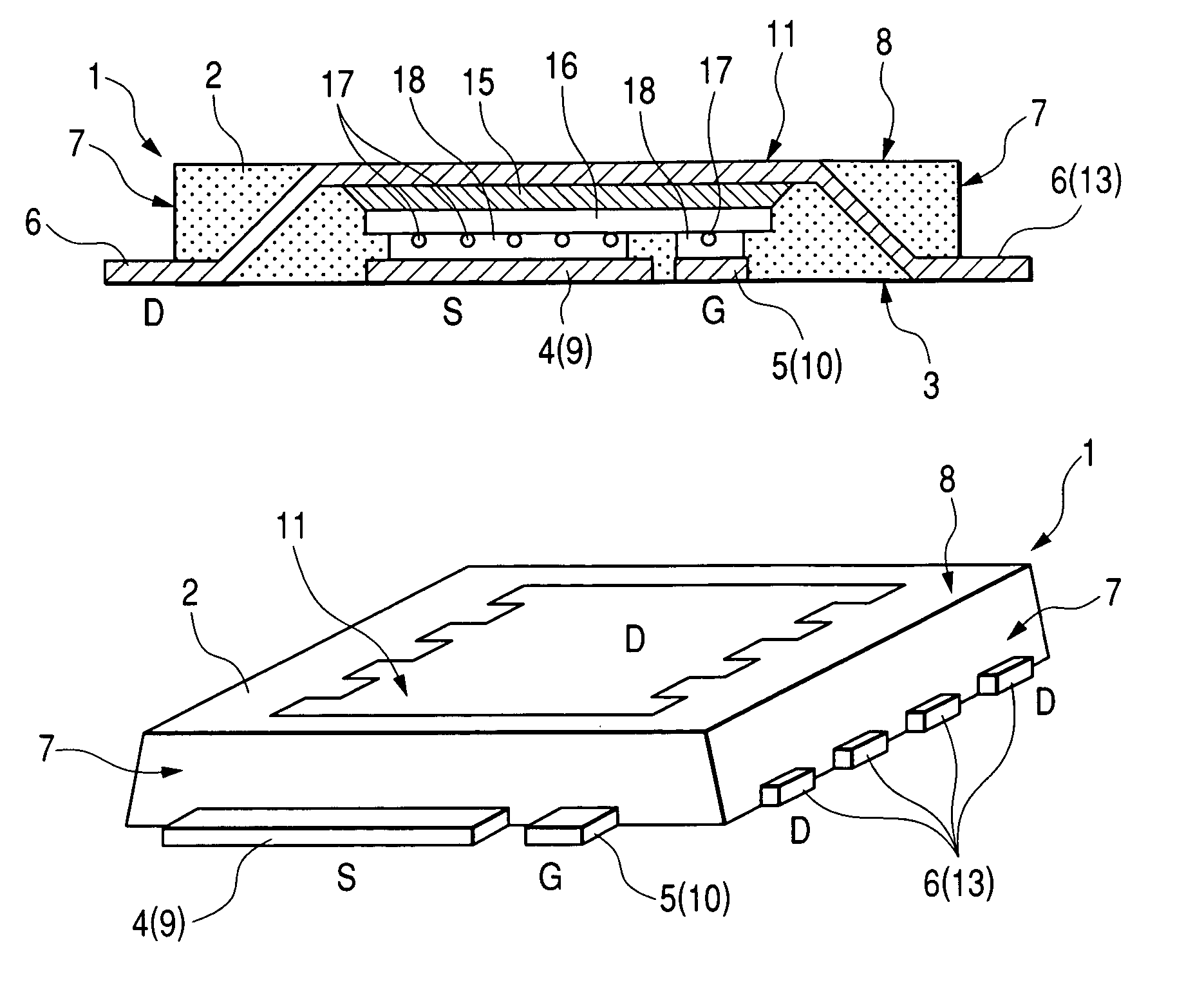
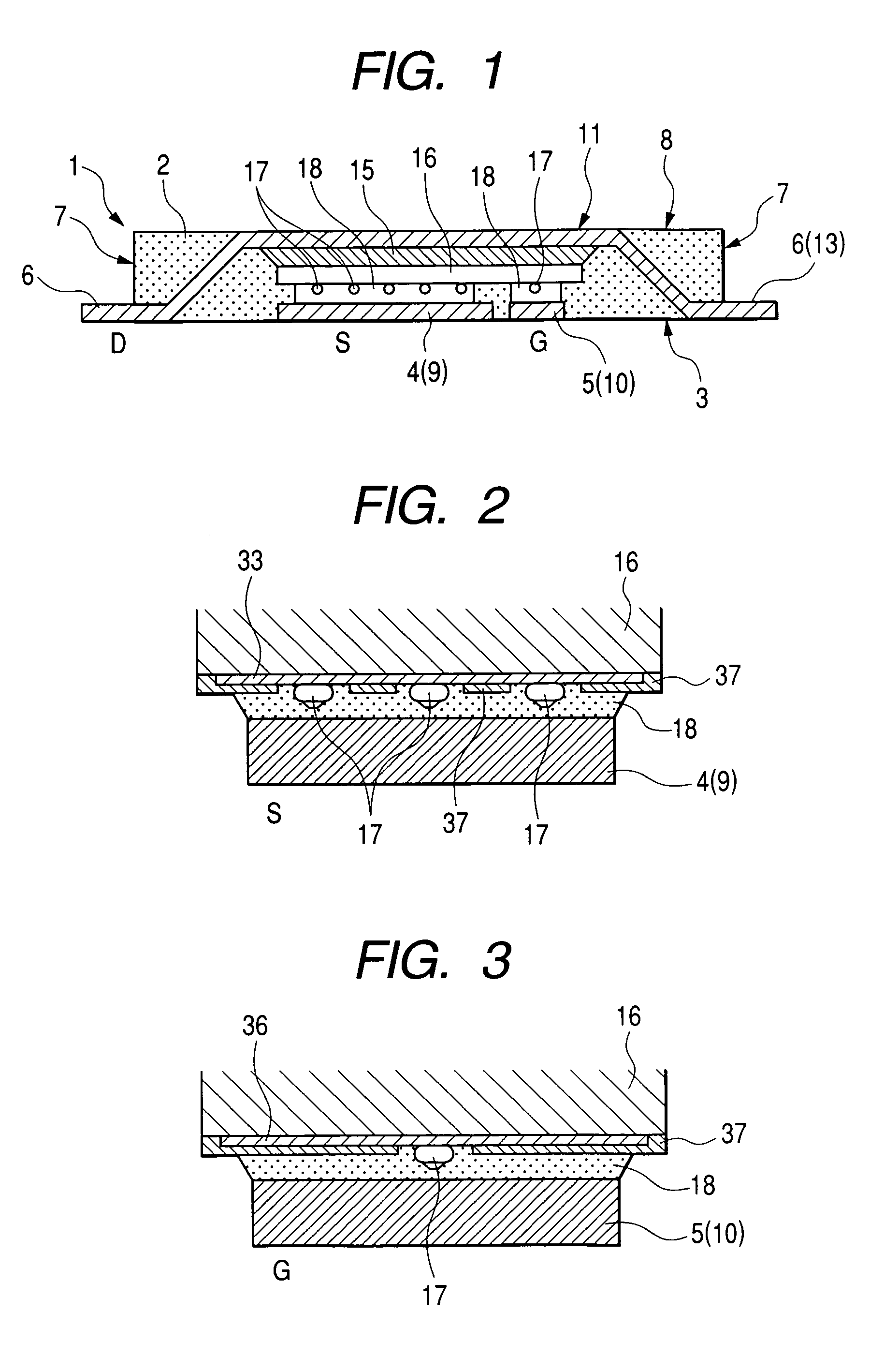
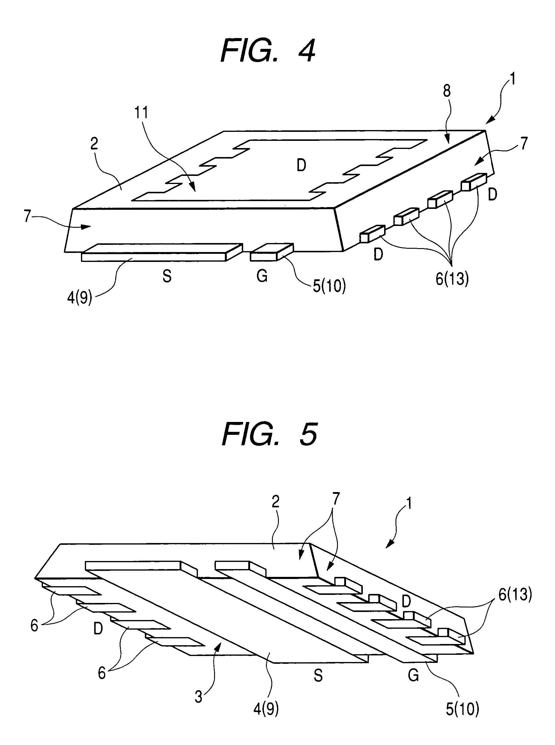
[0069]FIGS. 1 to 18(b) are concerned with a semiconductor device according to an embodiment (first embodiment) of the present invention, of which FIGS. 1 to 6 are related to the structure of the semiconductor device and FIGS. 7 to 18(b) are related to a method of manufacturing the semiconductor device.

[0070]In this first embodiment a description will be given of an example in which the present invention is applied to a power MOSFET device (semiconductor device). In the power MOSFET device is incorporated a semiconductor chip which forms a vertical power MOSFET. A source (S) electrode as a first electrode and a gate electrode (G) as a control electrode are provided on a first main surface of the semiconductor chip, while a drain (D) electrode as a second electrode is provided on a second main surface of the chip which is opposite to the first main surface.

[0071]As shown in FIGS. 1, 4 and 5, the power MOSFET device, indicated at 1, has a flat quadrangular sealing mem...

third embodiment

(Third Embodiment)

[0123]FIGS. 20 to 23 are related to a power MOSFET 1 according to a further embodiment (third embodiment) of the present invention, of which FIG. 20 is a schematic front view, FIG. 21 is a schematic plan view, FIG. 22 is a schematic side view, and FIG. 23 is a schematic bottom view, of the power MOSFET device 1.

[0124]In the power MOSFET 1 of this third embodiment, both ends of the electrode plate 13 in the power MOSFET device 1 of the first embodiment are not branched but the electrode plate 13 is used as a single drain electrode terminal 6. According to this structure, since both ends of the electrode plate 13 are flat, the area of heat dissipation increases and the heat dissipating performance of the power MOSFET device 1 is improved.

[0125]In this third embodiment, electrode plate portions projecting from side faces of the sealing member 2 are illustrated so as to be wider than the portion sealed with the sealing member. Actually, however, each electrode plate is...

fourth embodiment

(Fourth Embodiment)

[0126]FIGS. 24 to 29 illustrate a power MOSFET device 1 according to a further embodiment (fourth embodiment) of the present invention, of which FIG. 24 is a schematic front view, FIG. 25 is a schematic plan view, FIG. 26 is a schematic side view, FIG. 27 is a schematic bottom view, and FIG. 28 is a schematic sectional view, of the power MOSFET 1.

[0127]In the power MOSFET 1 of this fourth embodiment, the state of connection of the semiconductor 1 in the power MOSFET 1 of the first embodiment is reversed. More specifically, a flat electrode plate 85 having a lower surface exposed to the lower surface of the sealing member 2 is used as a drain electrode plate (drain electrode terminal 6). Further, two electrode plates 86 and 87 having upper surfaces exposed to the central portion of the upper surface 8 of the sealing member 2 and also having lower surfaces of end portions thereof exposed to a peripheral edge portion of the lower surface 3 of the sealing member 2 are...


PUM


Abstract

A semiconductor device to prevent breakage of a semiconductor chip is disclosed. The device incorporates a sealing member, a semiconductor chip and having a source and gate electrodes on a first main surface and a drain electrode on a second main surface, a first electrode plate having an upper surface exposed to an upper surface of the sealing member and a lower surface exposed to a lower surface of the sealing member, and second electrode plates each having a lower surface exposed to the lower surface of the sealing member. The drain electrode of the chip is electrically connected to the drain electrode plate through an adhesive. Stud type bump electrodes are formed by gold wire on the source and gate electrodes and are covered with an electrically conductive adhesive. The bump electrode(s) and the source and gate electrode plates are electrically connected with each other through the adhesive.

Description

CROSS-REFERENCE TO RELATED APPLICATION[0001]The present application claims priority from Japanese Patent application JP 2003-204732 filed on Jul. 31, 2003, the content of which is hereby incorporated by reference into this application.BACKGROUND OF THE INVENTION[0002]The present invention relates to a semiconductor device and a method of manufacturing the same. Particularly, the present invention is concerned with a technique applicable effectively to the manufacture of a semiconductor device in which a semiconductor chip having a power transistor is sealed.[0003]As a high output semiconductor device there is known a semiconductor device wherein a semiconductor chip having a power transistor such as, for example, a power MOSFET (Metal Oxide Semiconductor Field-Effect-Transistor), an IGBT (Insulated Gate Bipolar Transistor), or a bipolar power transistor is incorporated into a sealing member.[0004]A power MOSFET device has a structure wherein a power MOSFET chip is incorporated into ...

Claims


Application Information

Patent Timeline
Patent Type & Authority Patents(United States)
IPC IPC(8): H01L23/48H01L23/52H01L29/40H01L23/12H01L21/60H01L23/485H01L23/495
CPCH01L23/49562H01L24/33H01L24/13H01L24/11H01L24/83H01L2924/1305H01L2924/1306H01L2224/0401H01L2224/83192H01L2224/73204H01L2224/16245H01L2224/83139H01L2224/29111H01L2224/29139H01L2924/15747H01L2924/0132H01L2924/014H01L2924/01033H01L2924/01006H01L2224/05624H01L2224/0558H01L2924/13091H01L2924/13055H01L2924/0781H01L2924/01082H01L2924/01079H01L2224/1134H01L2224/13144H01L2224/32245H01L2224/73253H01L2224/838H01L2924/01005H01L2924/01013H01L2924/01015H01L2924/01029H01L2924/01047H01L2924/01078H01L2924/0105H01L2924/00014H01L2924/3512H01L2924/00H01L2924/181H01L2224/11H01L2224/13H01L2224/8314H01L2224/84138H01L24/05H01L2224/0603H01L2924/00012
Inventor HATA, TOSHIYUKISATO, HIROSHI
Owner RENESAS ELECTRONICS CORP
Why Eureka
Try Eureka