High density semiconductor memory cell and memory array using a single transistor and having counter-doped poly and buried diffusion wordline

Inactive Publication Date: 2006-01-31
SYNOPSYS INC
View PDF101 Cites 358 Cited by
  • Summary
  • Abstract
  • Description
  • Claims
  • Application Information

AI Technical Summary

Problems solved by technology

With 10 volts, this thus results in a substantial amount of time for programming a memory cell.
However, the application of a write voltage to the electrode of the gate controlled diode causes the silicon dioxide/silicon nitride interface to fill with positive charge, which is retained after the write operation is completed.
Accordingly, processes for flash devices tend to be one or two generations b

Method used


Image

  • High density semiconductor memory cell and memory array using a single transistor and having counter-doped poly and buried diffusion wordline
  • High density semiconductor memory cell and memory array using a single transistor and having counter-doped poly and buried diffusion wordline
  • High density semiconductor memory cell and memory array using a single transistor and having counter-doped poly and buried diffusion wordline

Examples


Embodiment Construction

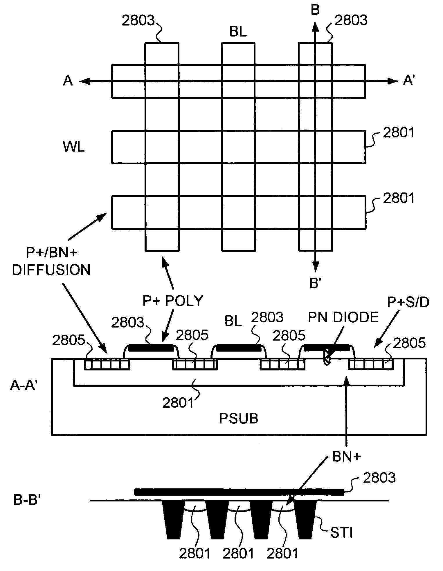
[0041]A semiconductor memory cell having a data storage element constructed around a gate oxide is used to store information by stressing the ultra-thin dielectric into breakdown (soft or hard breakdown) to set a leakage current level of the memory cell. The memory cell is read by sensing the current drawn by the cell. A suitable ultra-thin dielectric is the high quality gate oxide of about 10–50 Å thickness or less used in a transistor, as is commonly available from presently available advanced CMOS logic processes. Such oxides are commonly formed by deposition, by oxide growth from a silicon active region, or by some combination thereof. Other suitable dielectrics include oxide-nitride-oxide composites, compound oxides, and so forth.

[0042]In the following description, numerous specific details are provided to provide a thorough understanding of embodiments of the invention. One skilled in the relevant art will recognize, however, that the invention can be practiced without one or ...


PUM


Abstract

A programmable memory cell comprised of a transistor located at the crosspoint of a column bitline and a row wordline is disclosed. The transistor has its gate formed from the column bitline and its source connected to the row wordline. The memory cell is programmed by applying a voltage potential between the column bitline and the row wordline to produce a programmed p+ region to form a p-n diode in the substrate underlying the gate of the transistor. Further, the wordline is formed from a buried diffusion N+ layer while the column bitline is formed from a counterdoped polysilicon layer.

Description

RELATED APPLICATIONS[0001]This application is a continuation-in-part of U.S. patent application Ser. No. 10 / 765,802 filed Jan. 26, 2004 now U.S. Pat. No. 6,940,751 entitled “HIGH DENSITY SEMICONDUCTOR MEMORY CELL AND MEMORY ARRAY USING A SINGLE TRANSISTOR AND HAVING VARIABLE GATE OXIDE BREAKDOWN”, which is a continuation-in-part of U.S. patent application Ser. No. 10 / 677,613 filed Oct. 1, 2003 now U.S. Pat. No. 6,898,116 entitled “HIGH DENSITY SEMICONDUCTOR MEMORY CELL AND MEMORY ARRAY USING A SINGLE TRANSISTOR HAVING A BURIED N+ CONNECTION”, which is a continuation-in-part of U.S. patent application Ser. No. 10 / 448,505 filed May 30, 2003 now U.S. Pat. No. 6,856,540 entitled “HIGH DENSITY SEMICONDUCTOR MEMORY CELL AND MEMORY ARRAY USING A SINGLE TRANSISTOR” and U.S. patent application Ser. No. 10 / 133,704 filed Apr. 26, 2002 now U.S. Pat. No. 6,777,757 entitled “HIGH DENSITY SEMICONDUCTOR MEMORY CELL AND MEMORY ARRAY USING A SINGLE TRANSISTOR”, to which priority from all is hereby cl...

Claims


Application Information

Patent Timeline
IPC IPC(8): G11C11/34G11C17/12
CPCG11C17/12
Inventor PENG, JACK ZEZHONG
Owner SYNOPSYS INC
Why Eureka
Try Eureka