Optical filter device with aperiodically arranged grating elements

a filter device and aperiodic technology, applied in the direction of instruments, semiconductor lasers, cladded optical fibres, etc., can solve the problems of limiting the versatility of optical wdm communication systems, affecting the efficiency of optical aperiodic filter devices, etc., to achieve the effect of reducing the contrast, reducing the number of elements, and inefficient methods

Inactive Publication Date: 2006-01-31
ATOMERA INC
View PDF32 Cites 83 Cited by
  • Summary
  • Abstract
  • Description
  • Claims
  • Application Information

AI Technical Summary

Benefits of technology

[0012]According to one aspect of the invention, a method for creating an optical filter having aperiodically configured filter elements includes selecting initial characteristic attributes for the filter elements based upon a random seed, and generating an initial configuration of the filter elements having the characteristic attributes. A cost function is defined that represents a goodness of fit between a desired spectral response and a computed spectral response of the optical filter. The cost function is iteratively computed using a simulated annealing process by modifying at least one characteristic attribute of at least one filter element. If the iteratively computed cost function is less than a predetermined cost function, the configuration of the filter elements is selected as a desired configuration of the filter elements that corresponds to the iteratively computed cost function, thereby providing the desired spectral response.
[0013]According to another aspect of the invention, a method for producing an optical waveguide with a desired optical transmission characteristic includes defining a plurality of grating elements, wherein the grating elements represent an aperiodic grating, and selecting initial characteristic attributes for the grating elements based upon a random seed. An initial configuration of the grating

Problems solved by technology

However, the tuning range is in the order of 10 nm which is insufficient for optical WDM communication systems.
Conventional DBR laser grating designs typically employ deterministic gratings having a well-defined grating period which is smaller than the length of the grating, and other characteristic feature sizes, which limit their versatility.
The method, however, becomes inefficient for gratings having a greater number of eleme

Method used


Image

  • Optical filter device with aperiodically arranged grating elements
  • Optical filter device with aperiodically arranged grating elements
  • Optical filter device with aperiodically arranged grating elements

Examples


Embodiment Construction

[0027]The present invention will now be described more fully hereinafter with reference to the accompanying drawings, in which preferred embodiments of the invention are shown. This invention may, however, be embodied in many different forms and should not be construed as limited to the embodiments set forth herein. Rather, these embodiments are provided so that this disclosure will be thorough and complete, and will fully convey the scope of the invention to those skilled in the art. Like numbers refer to like elements throughout.

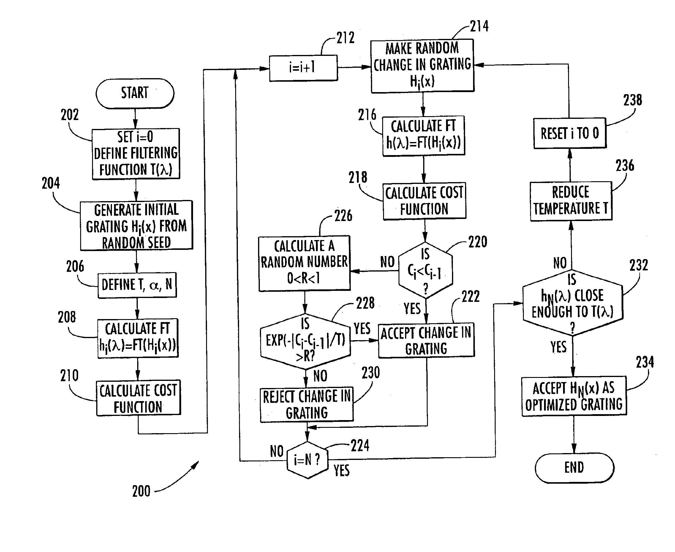
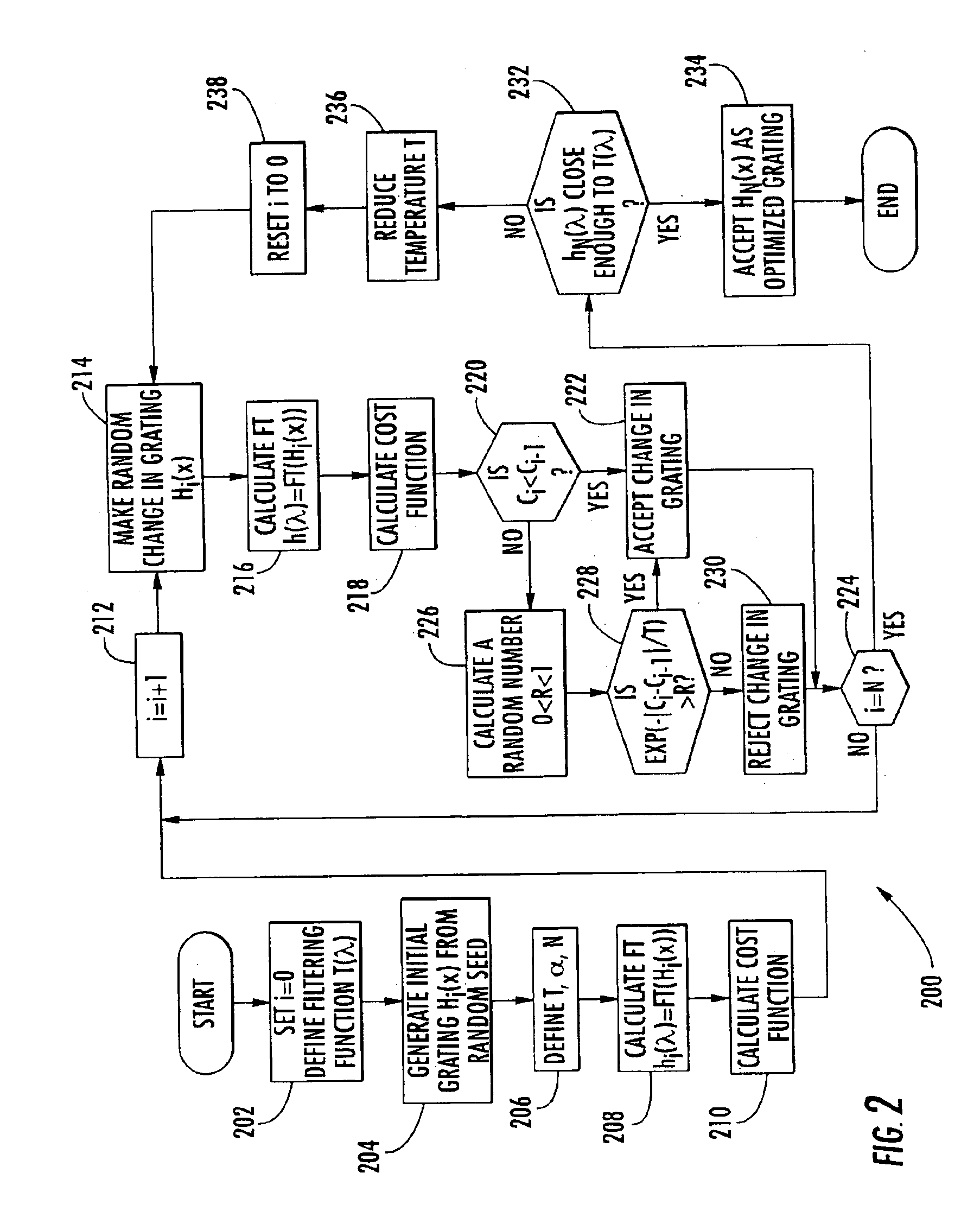
[0028]The method described herein is directed, inter alia, to an efficient algorithm for the design of aperiodic grating structures with a predetermined spectral response, such as a comb filter for applications as mirrors in optical waveguides and in DFB and DBR lasers. The structures described herein can be fabricated, for example, by electron-beam lithography and / or or photolithography using, for example, electron-beam-written masks.

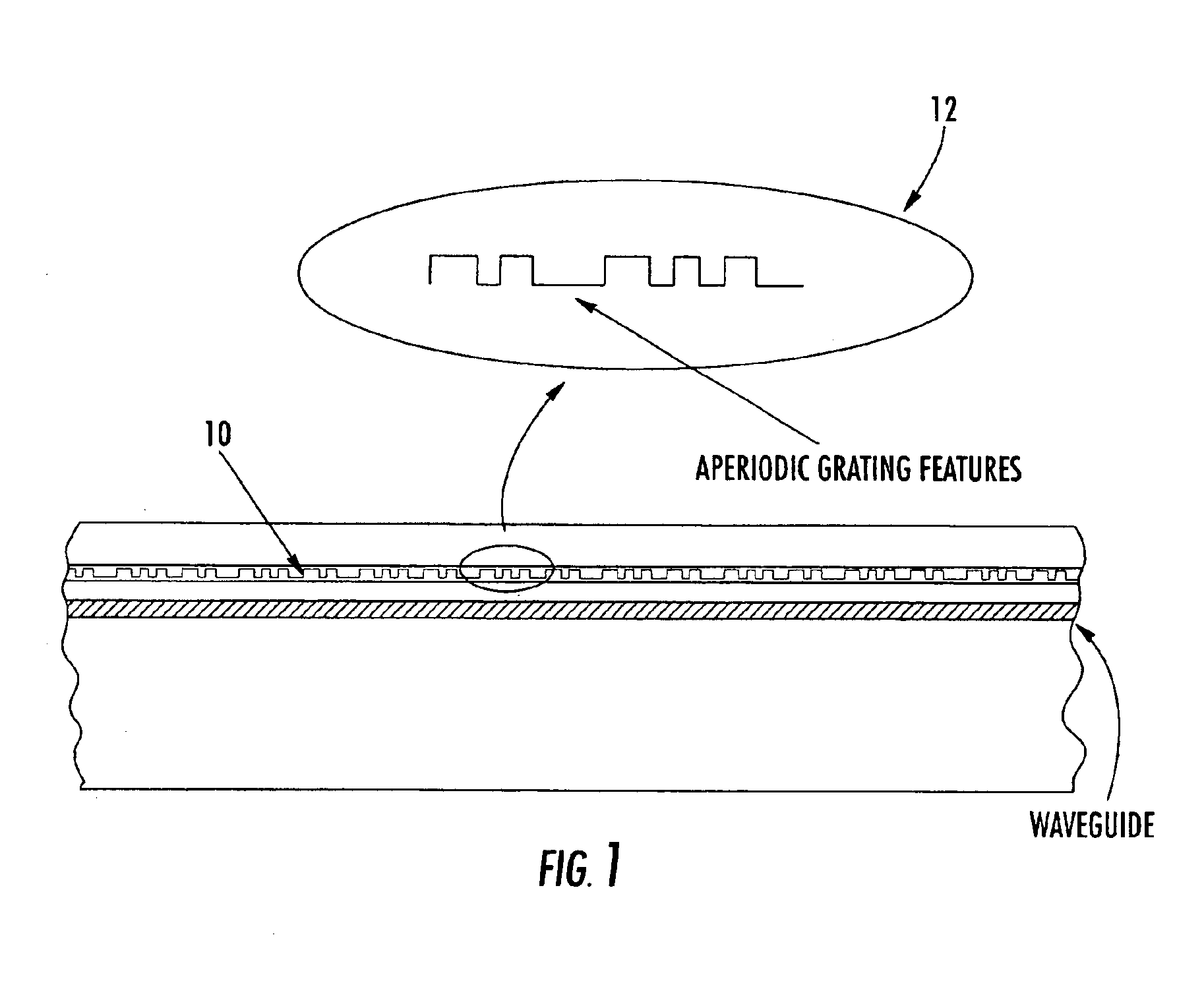
[0029]FIG. 1 illustra...


PUM


Abstract

A method for producing aperiodic gratings and waveguides with aperiodic gratings uses a simulated annealing process that starts with a random configuration of grating elements and iteratively computes a spectral response from a Fourier transform of the configuration of grating elements obtained in successive iterations. A cost function is computed as a convergence criterion. The aperiodic grating can be used, for example, as a filter in WDM applications.

Description

CROSS-REFERENCE TO RELATED APPLICATIONS[0001]This application is a continuation-in-part of U.S. patent application Ser. No. 09 / 914,944, filed Nov. 25, 2003, which is a national phase application of PCT / GB00 / 00768, filed Mar. 3, 2000, and claiming priority to British application 9905196.3, filed Mar. 3, 1999, the contents of which are incorporated herein by reference in their entirety.FIELD OF THE INVENTION[0002]The invention is directed to an optical aperiodic grating and filter structure producing multiple pass bands in either transmission or reflection. The grating / filter structure is designed by an efficient simulated annealing algorithm covering a large search space.BACKGROUND OF THE INVENTION[0003]Tunable multi-wavelength optical reflectors are important for a number of applications in optical telecommunications and signal processing including multiple channel optical telecommunications networks using wavelength division multiplexing (WDM). Such networks can provide advanced fe...

Claims


Application Information

Patent Timeline
IPC IPC(8): G02B6/34G02B6/02G02B6/124H01S5/12
CPCG02B6/02085G02B6/124H01S5/1206
Inventor MEARS, ROBERT J.PARKER, MICHAEL CHARLES
Owner ATOMERA INC
Why Eureka
Try Eureka