Spectrum simulation for semiconductor feature inspection

a semiconductor and feature inspection technology, applied in the direction of material analysis using wave/particle radiation, instruments, heat measurement, etc., can solve the problems of high processing defect rate, high complexity of semiconductor manufacturing process for integrating circuits into semiconductor materials, and high difficulty in detecting defects in semiconductor materials

Active Publication Date: 2006-02-07
KLA TENCOR TECH CORP
View PDF10 Cites 30 Cited by
  • Summary
  • Abstract
  • Description
  • Claims
  • Application Information

AI Technical Summary

Problems solved by technology

Generally, the semiconductor manufacturing industry involves highly complex techniques for integrating circuits into semiconductor materials.
Due to the large scale of circuit integration and the decreasing size of semiconductor devices, the semiconductor manufacturing process is prone to processing defects.
Semiconductor defects may include structural flaws, residual process material and other surface contamination, which occur during the production of semiconductor wafers.
As another example, a scratch defect may occur due to abrasive polishing during a chemical mechanical planarization process, or it may occur due to faulty cleaning process or it may occur from operator error during wafer handing.
Since defects can have a similar appearance but originate from different process steps, it can be difficult to find root causes of the defects, such as a faulty process.
Unfortunately, X-ray spectroscopy has certain inherent characteristics that effect the accuracy of measurements.
The resulting data therefore does not reflect accurately upon the defect since data relating to areas surrounding the defect is also included.

Method used


Image

  • Spectrum simulation for semiconductor feature inspection
  • Spectrum simulation for semiconductor feature inspection
  • Spectrum simulation for semiconductor feature inspection

Examples


Embodiment Construction

[0022]The present invention will now be described in detail with reference to a few preferred embodiments as illustrated in the accompanying drawings. In the following description, numerous specific details are set forth in order to provide a thorough understanding of the present invention. It will be apparent, however, to one skilled in the art, that the present invention may be practiced without some or all of these specific details. In other instances, well known operations have not been described in detail so not to unnecessarily obscure the present invention.

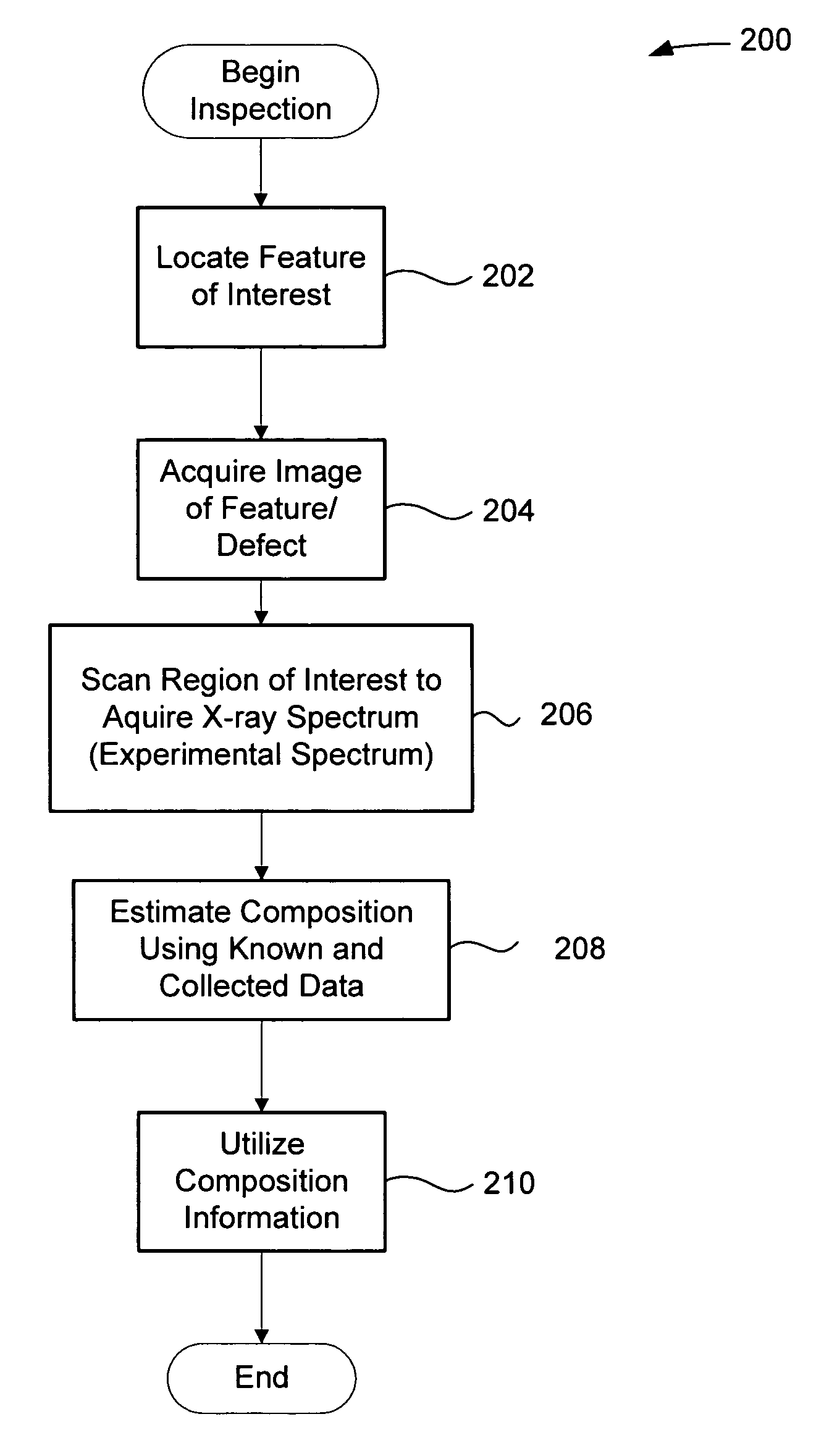
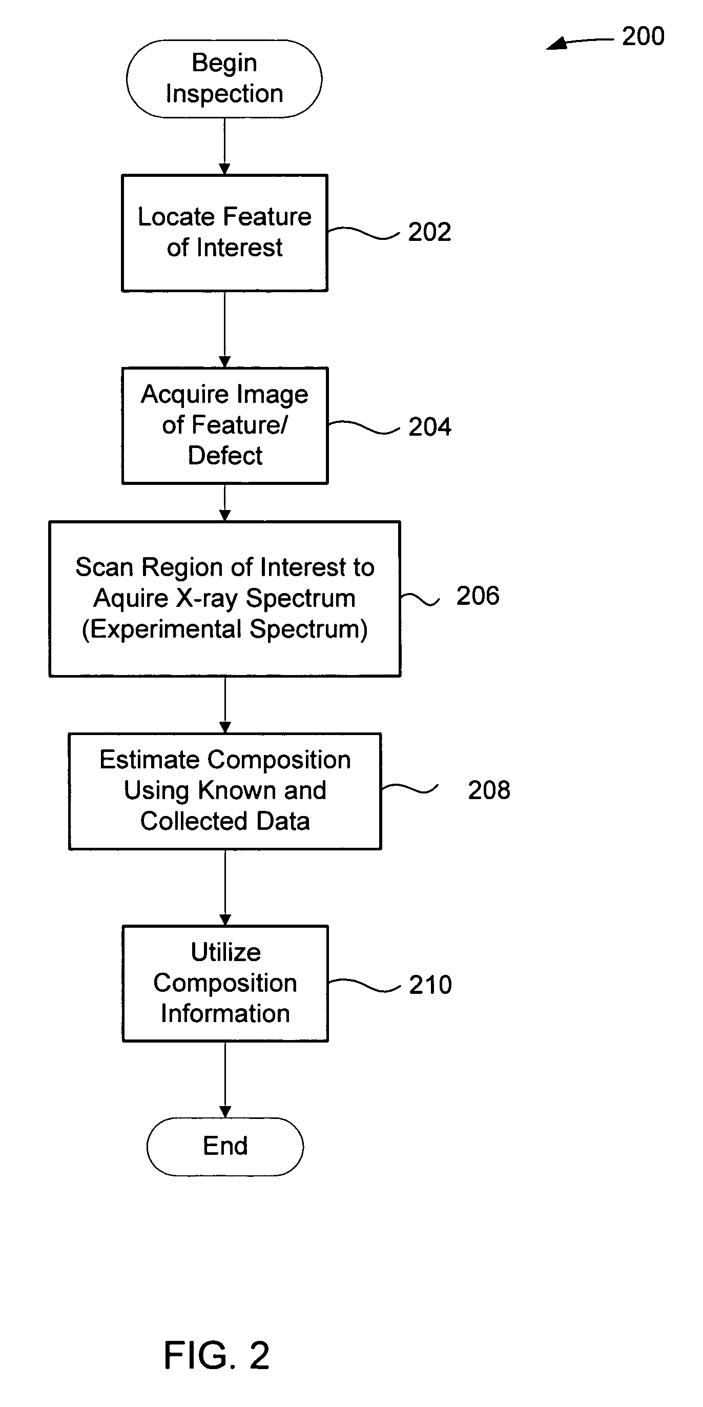
[0023]The present invention pertains to an application of X-ray spectroscopy to determine certain parameters of semiconductor specimens. For example, the invention can be used to determine parameters such as composition, dimensions, and density of semiconductor specimens. Specifically, an X-ray spectrum simulation algorithm is used to iteratively generate a theoretical X-ray spectrum for a semiconductor specimen having cert...


PUM

PropertyMeasurementUnit
atomic numbersaaaaaaaaaa
semiconductor inspectionaaaaaaaaaa
energy rangeaaaaaaaaaa

Abstract

Techniques for determining certain parameters of semiconductor specimens using X-ray spectroscopy are described. The invention can be used to determine parameters such as composition, dimensions, and density of semiconductor specimens. Specifically, an X-ray spectrum simulation algorithm is used to iteratively generate a theoretical X-ray spectrum for a semiconductor specimen having certain parameters. The iterative generation of theoretical X-ray spectrums continues until one of the theoretical X-ray spectrum closely matches the actual X-ray spectrum measured off of the specimen. In an alternative embodiment, this technique of generating theoretical X-ray spectrums can be used in combination with a pre-existing library of X-ray spectral signatures for semiconductor specimens having various parameters.

Description

CROSS-REFERENCE TO RELATED APPLICATIONS[0001]This application claims priority of U.S. provisional patent application No. 60 / 456,104, filed Mar. 18, 2003, entitled “Spectrum Simulation for Semiconductor Feature Inspection,” which is hereby incorporated by reference.FIELD OF THE INVENTION[0002]The present invention relates generally to semiconductor inspection techniques, and more specifically to such techniques that utilize x-ray spectroscopy.BACKGROUND OF THE INVENTION[0003]Generally, the semiconductor manufacturing industry involves highly complex techniques for integrating circuits into semiconductor materials. Due to the large scale of circuit integration and the decreasing size of semiconductor devices, the semiconductor manufacturing process is prone to processing defects. Semiconductor defects may include structural flaws, residual process material and other surface contamination, which occur during the production of semiconductor wafers. Defects can be introduced to a wafer a...

Claims


Application Information

Patent Timeline
Patent Type & Authority Patents(United States)
IPC IPC(8): G01K11/30
CPCG01N23/2252
Inventor TESTONI, ANNE L.
Owner KLA TENCOR TECH CORP
Why Eureka
Try Eureka