Soldering structure between a tab of a bus bar and a printed substrate

a technology of printed substrate and soldering structure, which is applied in the direction of printed circuit, fixed connection, coupling device connection, etc., can solve the problems of number of components, working steps, and electrical conductive material , so as to reduce the cost and the working process greatly, avoid the effect of applying

Inactive Publication Date: 2006-02-14
SUMITOMO WIRING SYST LTD
View PDF7 Cites 12 Cited by
  • Summary
  • Abstract
  • Description
  • Claims
  • Application Information

AI Technical Summary

Benefits of technology

[0014]As described above, in the case where the tab of the bus bar intersects the electrical conductive material on the printed substrate in perpendicular to each other, because the stress-absorbing aperture or recess formed in the insulation plate at the position immediately below the tab absorbs a difference in coefficients of extension between the tab and the electrical conductive material when the flowing current generates heat, it is possible to avoid applying a stress to the soldered portion.
[0015]Consequently, a connector connection is not required and a simple soldering process can reduce a cost and a working process greatly.

Problems solved by technology

If this stress increases, the soldered portion between the tab 2b and the electrical conductive material 4 tends to cause cracks.
However, this connecting means using the connector will increase the number of components and working steps and will further bring the ECU and printed substrate into a large size.

Method used


Image

  • Soldering structure between a tab of a bus bar and a printed substrate
  • Soldering structure between a tab of a bus bar and a printed substrate
  • Soldering structure between a tab of a bus bar and a printed substrate

Examples


Embodiment Construction

[0020]Referring now to the drawings, embodiments of a soldering structure between a tab of a bus bar and a printed substrate in accordance with the invention will be described below.

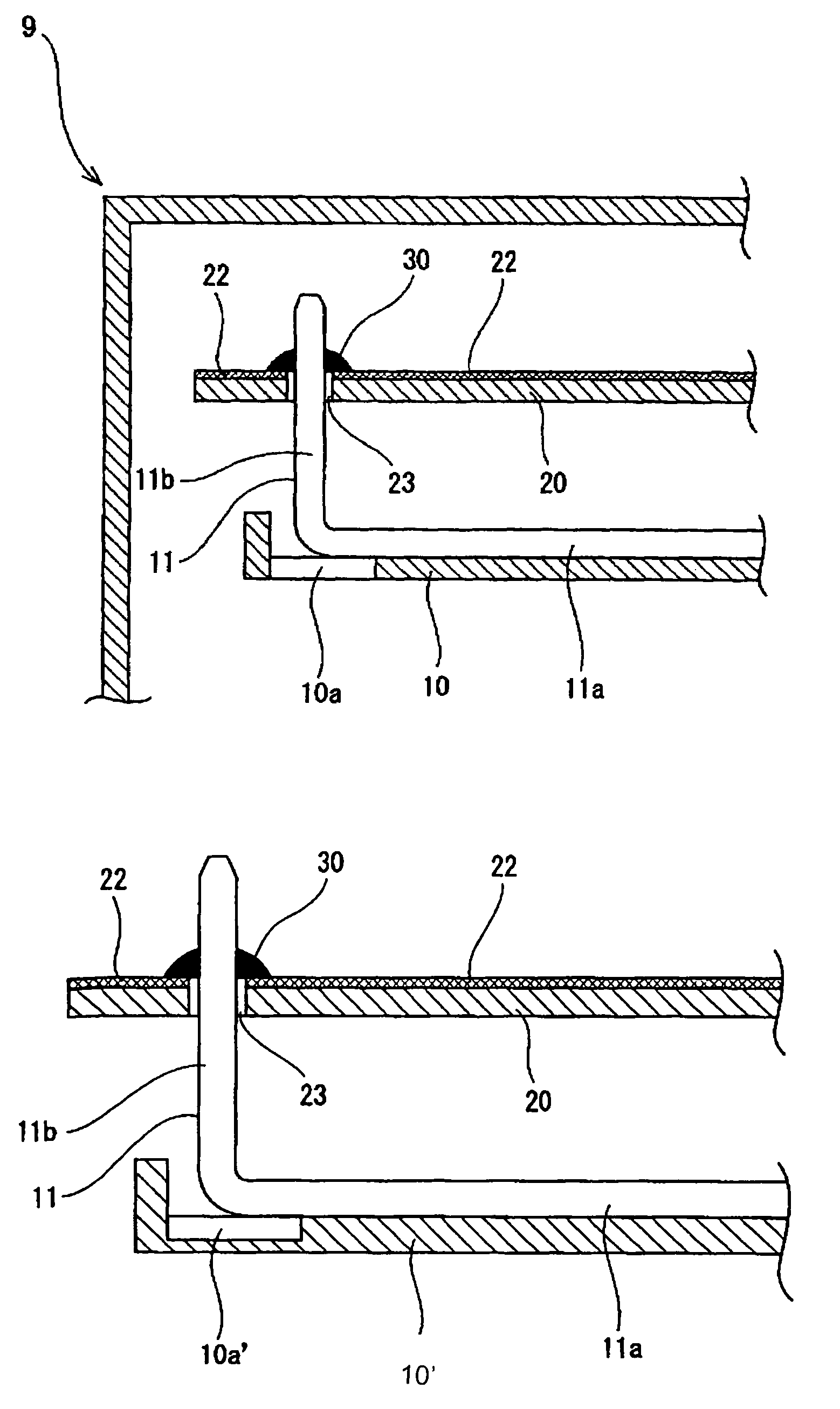
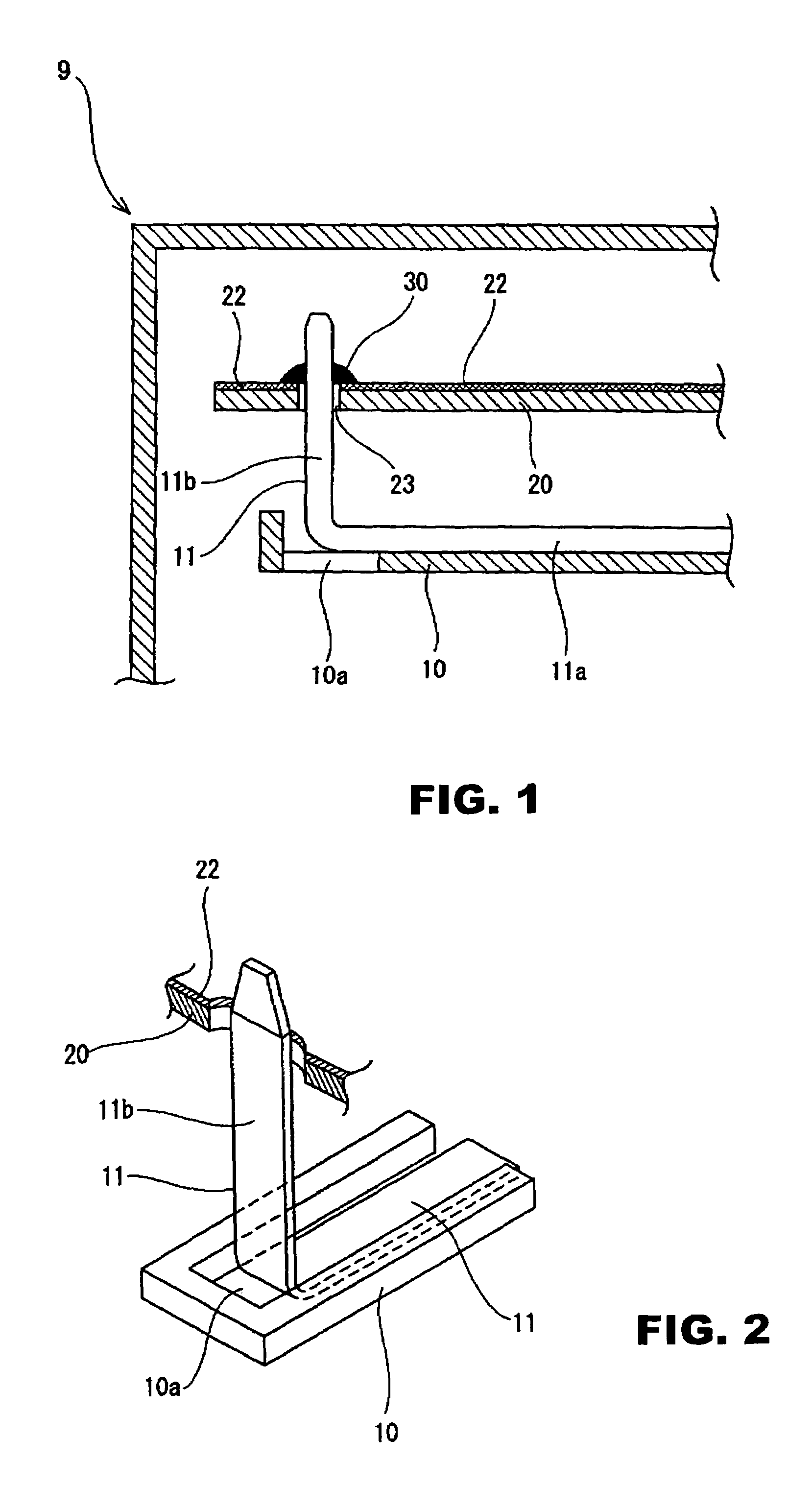
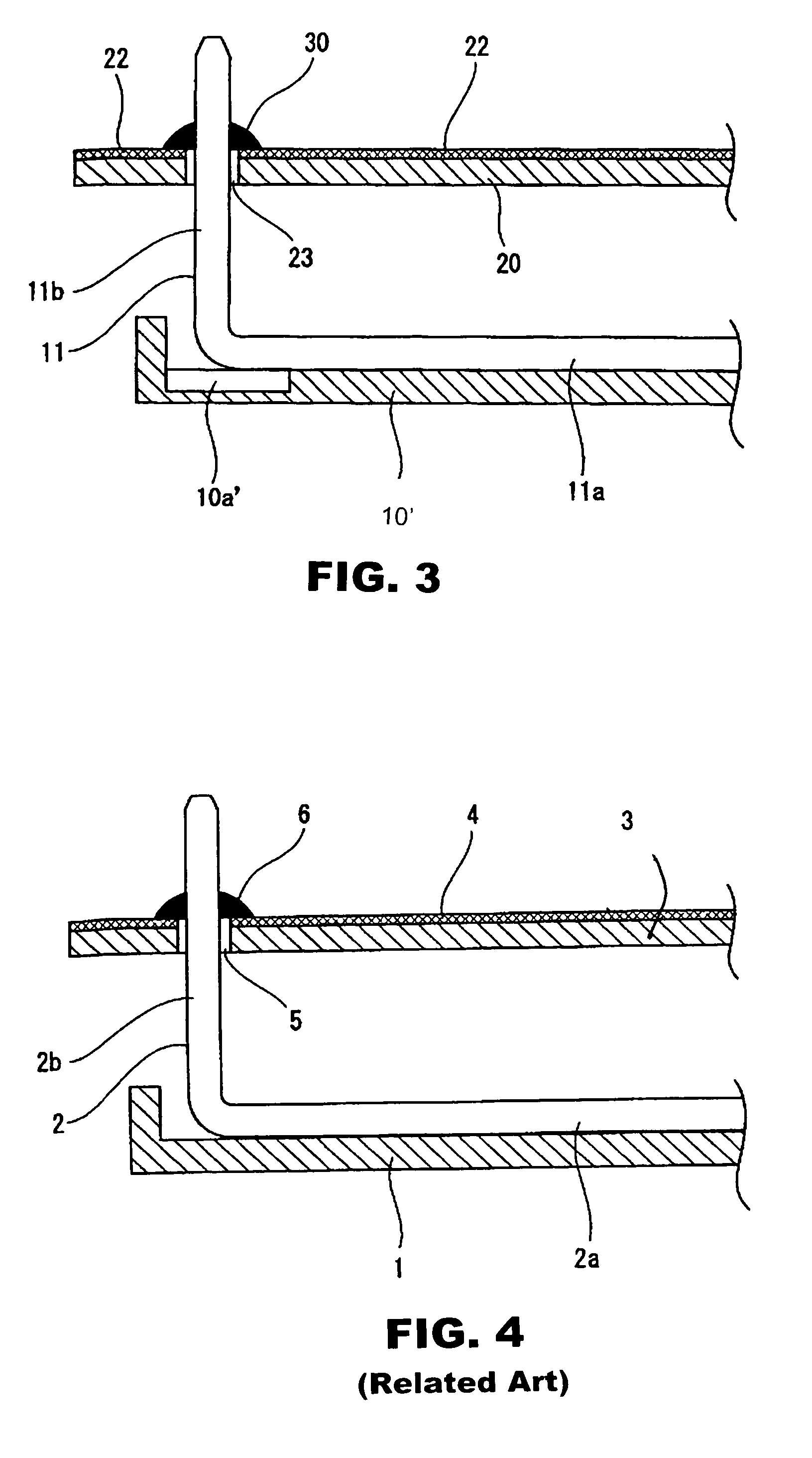
[0021]FIGS. 1 and 2 show a first embodiment of a soldering structure between a tab of a bus bar and a printed substrate in accordance with the invention. A bus bar 11 punched out from a brass plate is mounted on an insulation plate 10 in a horizontal direction and they are contained in an electrical junction box 9 to be mounted on an automobile vehicle. A printed substrate 20 is contained above the bus bar 11 in the electrical junction box 9. The bus bar 11 and printed substrate 20 are located in a layered manner in a vertical direction in the box 9.

[0022]A horizontal body 11a of the bus bar 11 is mounted on the insulation plate 10. A tab 11b is formed by bending an end of the body 11a upward. A stress-absorbing aperture 10a is provided in the insulation plate 10 immediately below a proximal end (lower e...


PUM


Abstract

A soldering structure between a tab of a bus bar and a printed substrate is disclosed to provide a soldering structure between a tab of a bus bar and a printed substrate that causes no crack. An electrical conductive material is formed on a printed substrate. A tab through-hole is provide to penetrate the electrical conductive material and printed substrate. A tab formed by bending a body of the bus bar enters the tab through-hole. A periphery of the tab and the electrical conductive material are interconnected by soldering. A stress-absorbing aperture or recess is provided in an insulation plate on which the body of the bus bar is mounted. The stress-absorbing aperture or recess can absorb an axial stress caused in the tab.

Description

CLAIM FOR PRIORITY[0001]This invention relates to subject-matter contained in and claims priority to JP 2003-301935, filed on Aug. 26, 2003, the entire disclosure of which is incorporated herein by reference thereto.BACKGROUND OF THE INVENTION[0002]1. Field of Invention[0003]This invention relates to a soldering structure between a tab of a bus bar and a printed substrate. More particularly, in the case where the printed substrate and bus bar are contained in a layered manner in an electrical junction box to be mounted on an automobile vehicle, and where the tab of the bus bar is soldered on an electrical conductive material on the printed substrate so that the tab intersects the electrical conductive material in a vertical direction, the soldered portion can be prevented from causing cracks.[0004]2. Description of Related Art[0005]As electrical components to be mounted on an automobile vehicle increase, a printed substrate constituting an ECU (Electronic Control Unit) together with...

Claims


Application Information

Patent Timeline
Patent Type & Authority Patents(United States)
IPC IPC(8): H01R13/58H01R4/02H01R12/55H01R43/02H02G3/16H05K3/20H05K3/34H05K7/06
CPCH01R9/091H05K3/3447H01R43/0256H05K3/202H01R12/7088H05K2201/09063H05K2201/10272H05K2201/10757Y10S439/949H05K2201/0397H01R12/58
Inventor HIWATASHI, HIROKAZU
Owner SUMITOMO WIRING SYST LTD
Why Eureka
Try Eureka