Bandgap reference voltage circuit

a reference voltage and circuit technology, applied in the direction of electric variable regulation, process and machine control, instruments, etc., can solve the problems of bandgap reference voltage overshooting its intended value, vref to drift, and start-up operation (the pulling of nodes b>518/b> and b>519/b> up and down) may end too early or too late, so as to reduce the dependence of constant current and high reliability

Inactive Publication Date: 2006-02-14
LAPIS SEMICON CO LTD
View PDF19 Cites 28 Cited by
  • Summary
  • Abstract
  • Description
  • Claims
  • Application Information

AI Technical Summary

Benefits of technology

[0025]Providing the power supply voltage detection circuit with circuit elements similar to circuit elements in the constant-current circuit enables the power supply voltage detection circuit to detect with high reliability whether or not the power supply has reached the lower limit voltage and end the start-up operation at the proper time.
[0026]The start-up output circuit has a node that controls the supply of the starting potential to the starter node in the constant-current circuit. After the lower limit voltage has been reached, this node is preferably connected by a low-impedance path to the power supply, so that power-supply noise does not trigger the unwanted further supply of the starting potential to the starter node.
[0027]The constant-current circuit may include a negative feedback loop that reduces the dependence of the constant current on the voltage of the power supply.

Problems solved by technology

Noise in the low power supply Vss can also cause Vref to drift.
One problem is that, depending on the temperature characteristics of the circuit elements and the speed at which the high power supply Vcc rises when power is initially applied, the start-up operation (the pulling of nodes 518 and 519 up and down) may end too early or too late.
If the start-up operation continues too long after Vcc reaches the necessary level, the bandgap reference voltage may overshoot its intended value, and power is needlessly consumed.
Another problem is that transistors P516, P518, and P520 in start-up circuit 60A form a path through which unwanted current flows during steady-state operation.
The bandgap reference voltage circuit shown in FIG. 21 thus lacks inherent immunity from power-supply noise.

Method used


Image

  • Bandgap reference voltage circuit
  • Bandgap reference voltage circuit
  • Bandgap reference voltage circuit

Examples


first embodiment

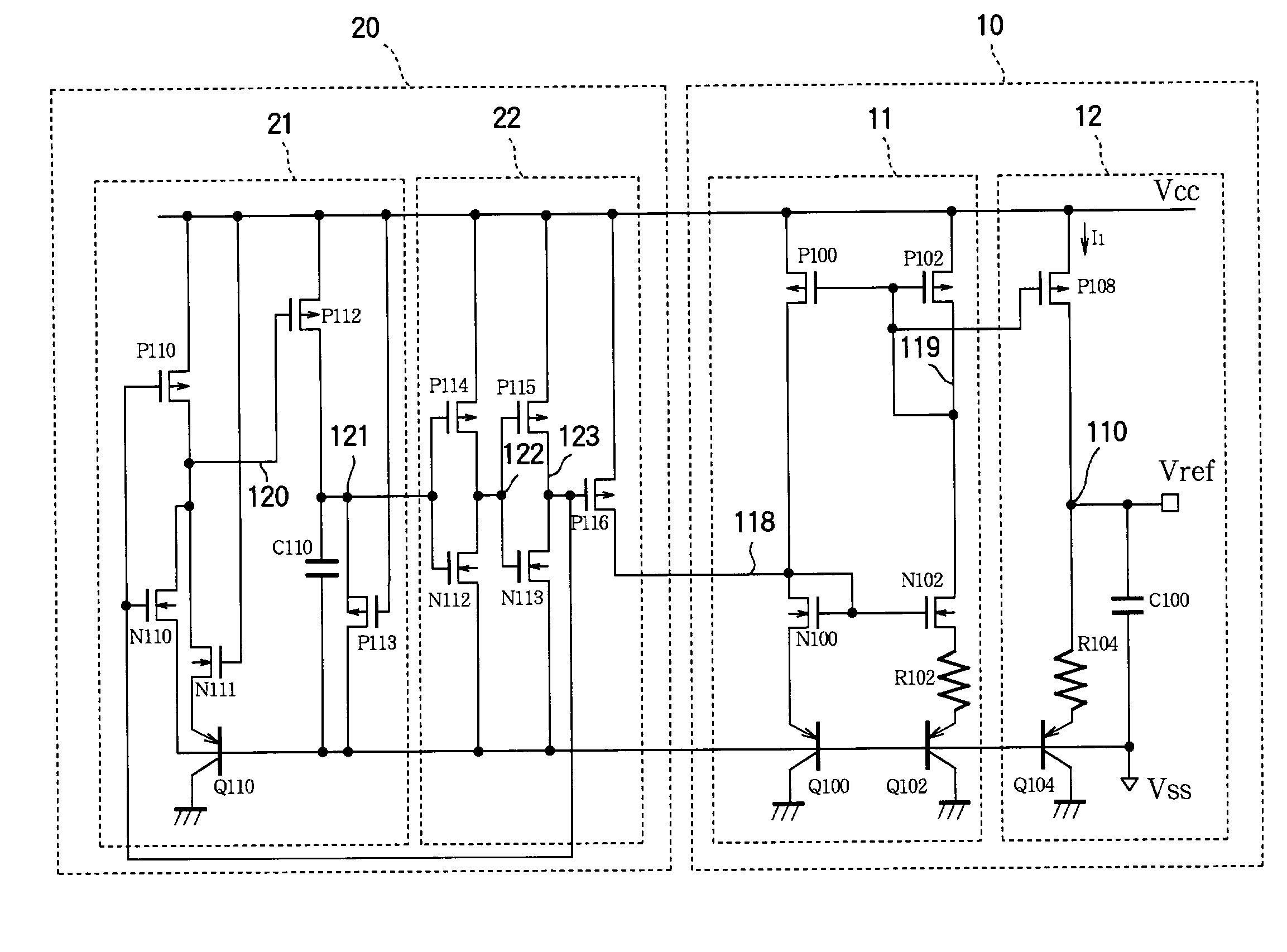
[0051]FIG. 1 is a circuit diagram of a bandgap reference voltage circuit illustrating a first embodiment of the invention. This bandgap reference voltage circuit comprises a reference stage 10 and a start-up stage 20. The reference stage 10 generates a constant current proportional to a thermal voltage, and generates a bandgap reference voltage from the constant current. The start-up stage 20 starts the reference stage 10 when power is initially applied.

Structure of the Reference Stage 10

[0052]The reference stage 10 comprises a constant-current circuit11 and a bandgap reference voltage output circuit 12. The constant-current circuit 11 generates a constant current I1 proportional to a thermal voltage. The bandgap reference voltage output circuit 12 generates a bandgap reference voltage Vref from the constant current I1.

[0053]The constant-current circuit 11 comprises a first pair of p-channel metal-oxide-semiconductor (MOS) transistors P100 and P102, a second pair of p-channel MOS tr...

second embodiment

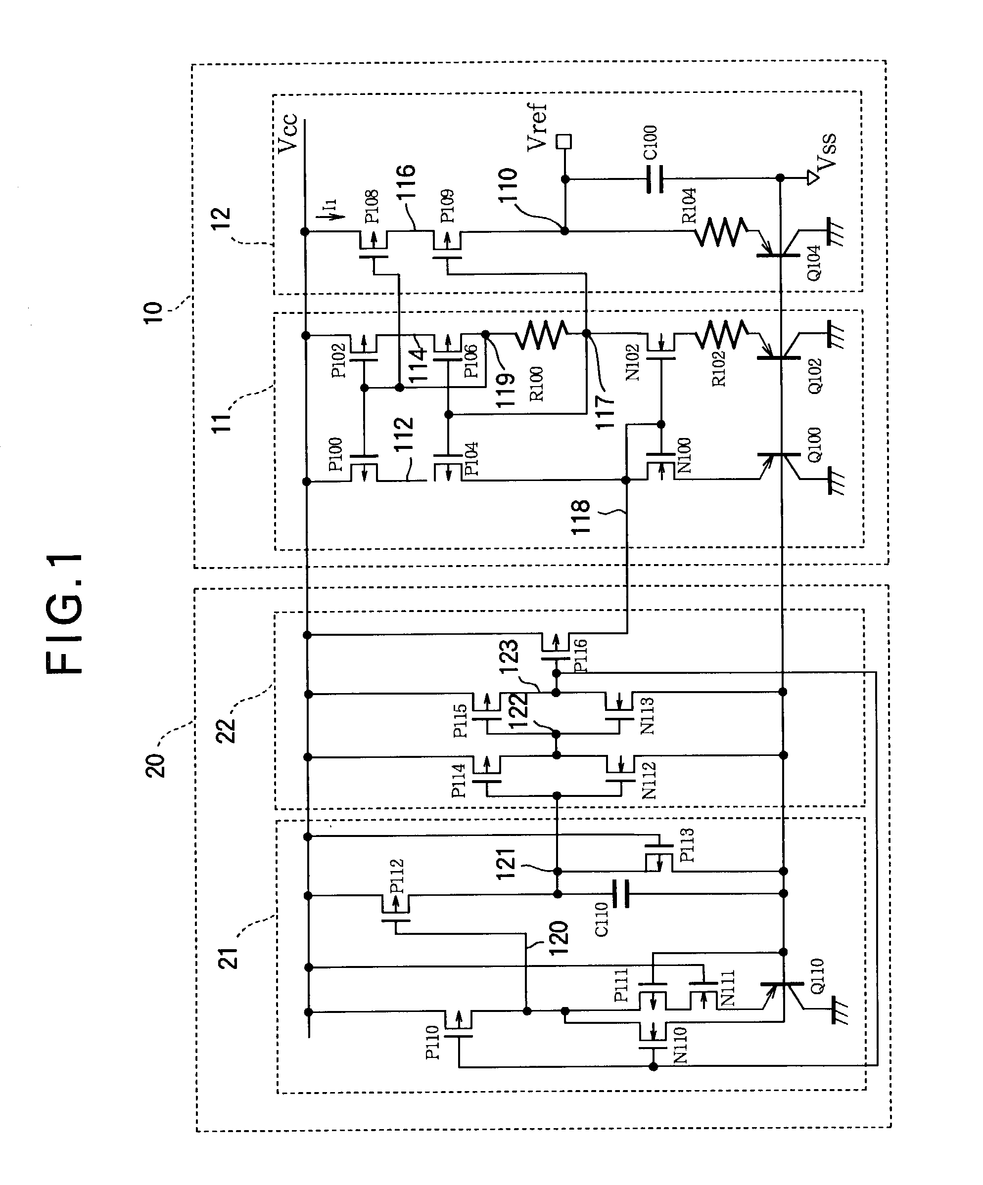
[0095]FIG. 5 is a circuit diagram of a bandgap reference voltage circuit illustrating a second embodiment of the invention, this embodiment also comprising a reference stage 10 and a start-up stage 20. The reference stage 10 has the same configuration as in the first embodiment; the start-up stage 20 has a different configuration.

Structure of the Start-Up Stage 20

[0096]In the start-up stage 20 shown in FIG. 5, the power supply voltage detection circuit 21 comprises p-channel transistors P111 and P112 and n-channel transistor N110. The source of transistor N110 is coupled to the low power supply Vss. Transistors P111 and P112 are connected in series between the high power supply Vcc and node 120, which is coupled to the drain of transistor N110. The gates of transistors P111 and P112 are coupled to the low power supply Vss.

[0097]The power supply voltage detection circuit 21 in FIG. 5 also comprises n-channel transistors N111, N115, and N117, pnp bipolar transistor Q110, and capacitor...

third embodiment

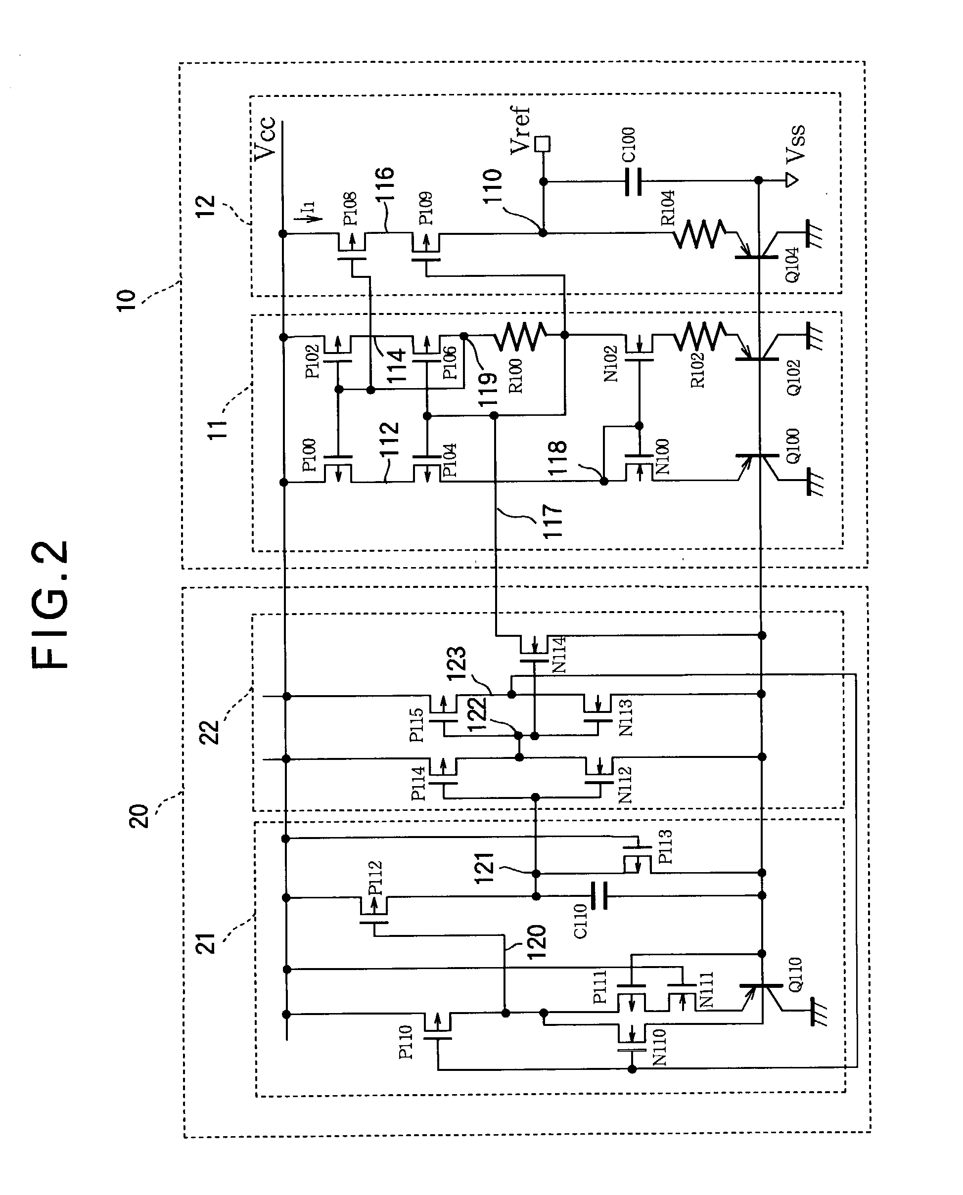
[0128]FIG. 9 is a circuit diagram of a bandgap reference voltage circuit illustrating a third embodiment of the invention, this embodiment also comprising a reference stage 10 and a start-up stage 20. The start-up stage 20 has the same configuration as in the first embodiment, while the reference stage 10 has a different configuration.

[0129]The reference stage 10 comprises a constant-current circuit 11 and a bandgap reference voltage output circuit 12. The bandgap reference voltage output circuit 12 has the same configuration as in the first embodiment (see FIG. 1), while the constant-current circuit 11 has a different configuration.

Structure of the Reference Stage 10

[0130]The constant-current circuit 11 in the third embodiment differs from the constant-current circuit 11 in the preceding embodiments by including a third current path and a negative feedback loop. Specifically, the constant-current circuit 11 in FIG. 9 comprises a first triad of p-channel transistors P100, P101, and ...


PUM


Abstract

A bandgap reference voltage circuit includes a constant-current circuit, a reference voltage output circuit generating a reference voltage according to the constant current, a power supply voltage detection circuit, and a start-up output circuit. The start-up output circuit supplies a starting potential to the constant-current circuit until the power supply voltage detection circuit detects that the power supply has reached a voltage sufficient for the constant-current circuit to maintain operation. The power supply voltage detection circuit has elements analogous to the elements in the constant-current circuit that determine this voltage, so start-up operation can occur and end reliably. The start-up output circuit includes a low-impedance path from the power supply to a node controlling supply of the starting potential, so power-supply noise does not trigger unwanted output of the starting potential after start-up operation has ended.

Description

BACKGROUND OF THE INVENTION[0001]1. Field of the Invention[0002]The present invention relates to a circuit for generating a reference voltage, more particularly to a bandgap reference voltage circuit.[0003]2. Description of the Related Art[0004]Bandgap reference voltage circuits are widely used because of their ability to generate a reference voltage that does not vary with temperature. FIG. 21 shows a bandgap reference voltage circuit described in, for example, Japanese Unexamined Patent Application Publication No. 11-231948. The circuit includes a reference stage 50 that generates a constant current proportional to a thermal voltage and generates the bandgap reference voltage from the constant current, a pair of start-up circuits 60A, 60B that start the reference stage 50 when power is initially applied, and a pair of filters 70A, 70B that filter the high power supply Vcc and lower power supply Vss.[0005]During operation, p-channel transistors P500, P502, P508 form a first current...

Claims


Application Information

Patent Timeline
Patent Type & Authority Patents(United States)
IPC IPC(8): G05F1/10G05F3/30G05F3/24
CPCG05F3/30
Inventor SUGIMURA, NAOAKI
Owner LAPIS SEMICON CO LTD
Why Eureka
Try Eureka