Systems for electroplating metal onto a layer of low conductivity material

Inactive Publication Date: 2006-02-21
MICRON TECH INC
View PDF7 Cites 0 Cited by
  • Summary
  • Abstract
  • Description
  • Claims
  • Application Information

AI Technical Summary

Benefits of technology

[0014]By virtue of the ability to vary the amplitude and duration of the applied potential or current pulse, the method facilitates the filling of structures in the center of the low conductivity layer without overdepositing on the outside edge, thus ensuring a predetermined profile of deposited material across the entire surface of the low conductivity layer.

Problems solved by technology

Various difficulties are associated with the electroplating of metals such as copper onto low conductivity barrier materials such as Ta and W. In the context of semiconductor fabrication, the major problem associated with plating on such barriers is that of achieving the required adhesion and uniformity of the electroplated layer across the surface of a wafer without the presence of fill defects.
While conventional pulse plating techniques can enable conformal plating across a surface under certain circumstances, for the following reason these techniques are not always effective for plating a resistive layer.
Therefore, with conventional techniques, the electroplated deposits are typically excessively thick at the edge of an object, such as a wafer, with minimal deposition at the center.
While the use of a high pulse amplitude may provide a more uniform deposit, it will also lead to filling problems in the high aspect ratio features common to semiconductor processes.
Electroplating a layer of metal on a layer of low conductivity material, however, presents another obstacle.

Method used


Image

  • Systems for electroplating metal onto a layer of low conductivity material
  • Systems for electroplating metal onto a layer of low conductivity material
  • Systems for electroplating metal onto a layer of low conductivity material

Examples


Embodiment Construction

[0024]The present invention will be understood from the exemplary embodiments described herein.

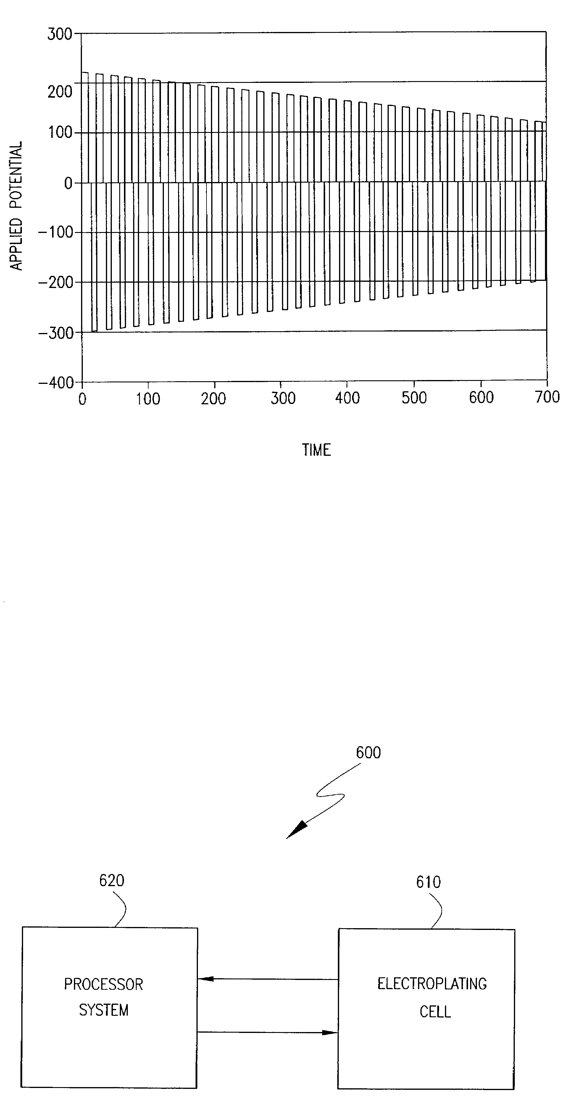
[0025]The present invention relates to a method of electroplating metal onto a layer of low conductivity material. The method is particularly useful for the filling of structures in the center surface of the low conductivity layer without overdepositing on the outside edge, thus ensuring a controlled profile from deposition of the material across the entire surface of the low conductivity layer. The method provides a structure, such as for example, a semiconductor wafer or a chip produced therefrom, comprising a substrate, a low conductivity layer, and a uniform layer of electroplated metal deposited on the low conductivity layer.

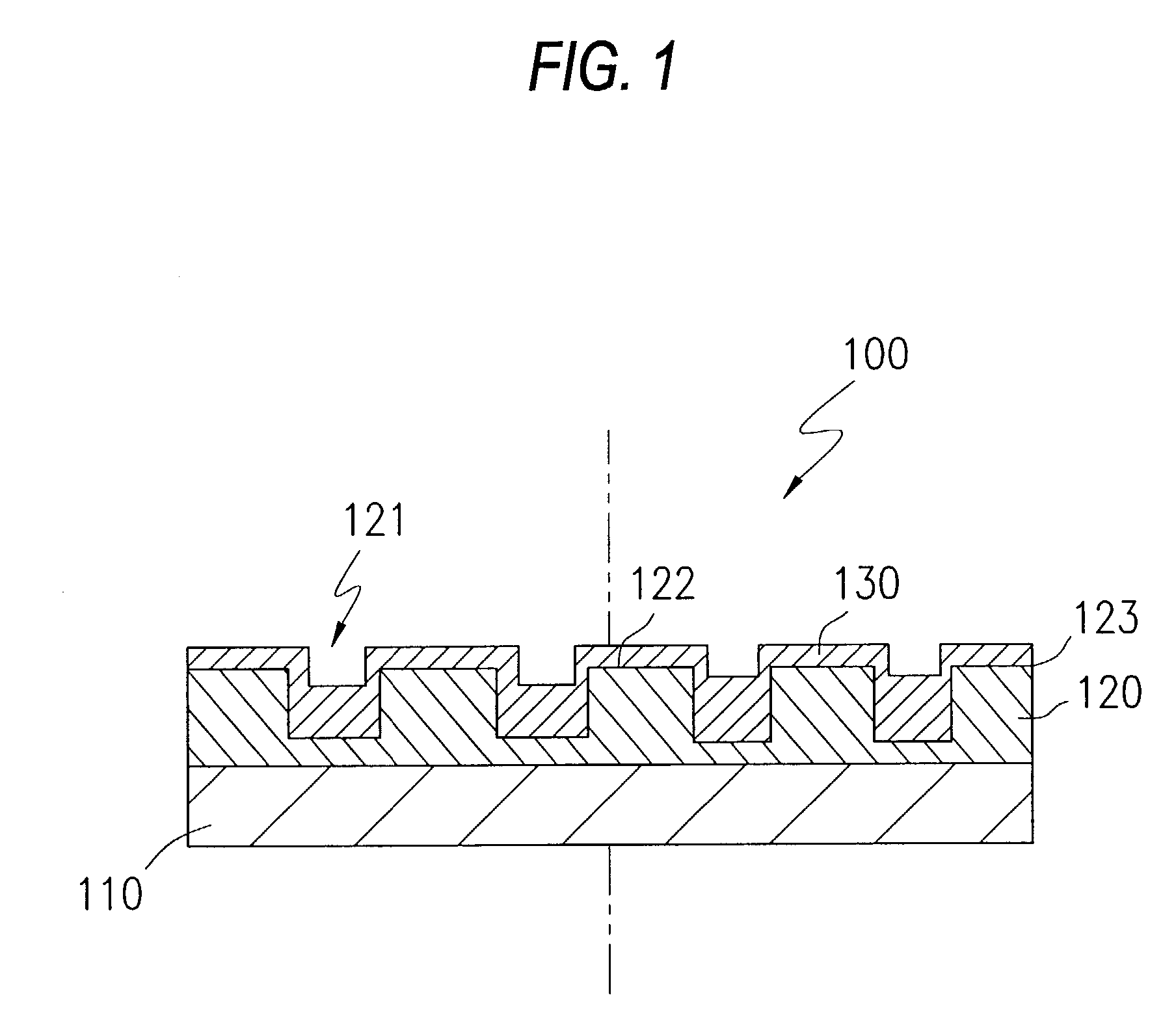
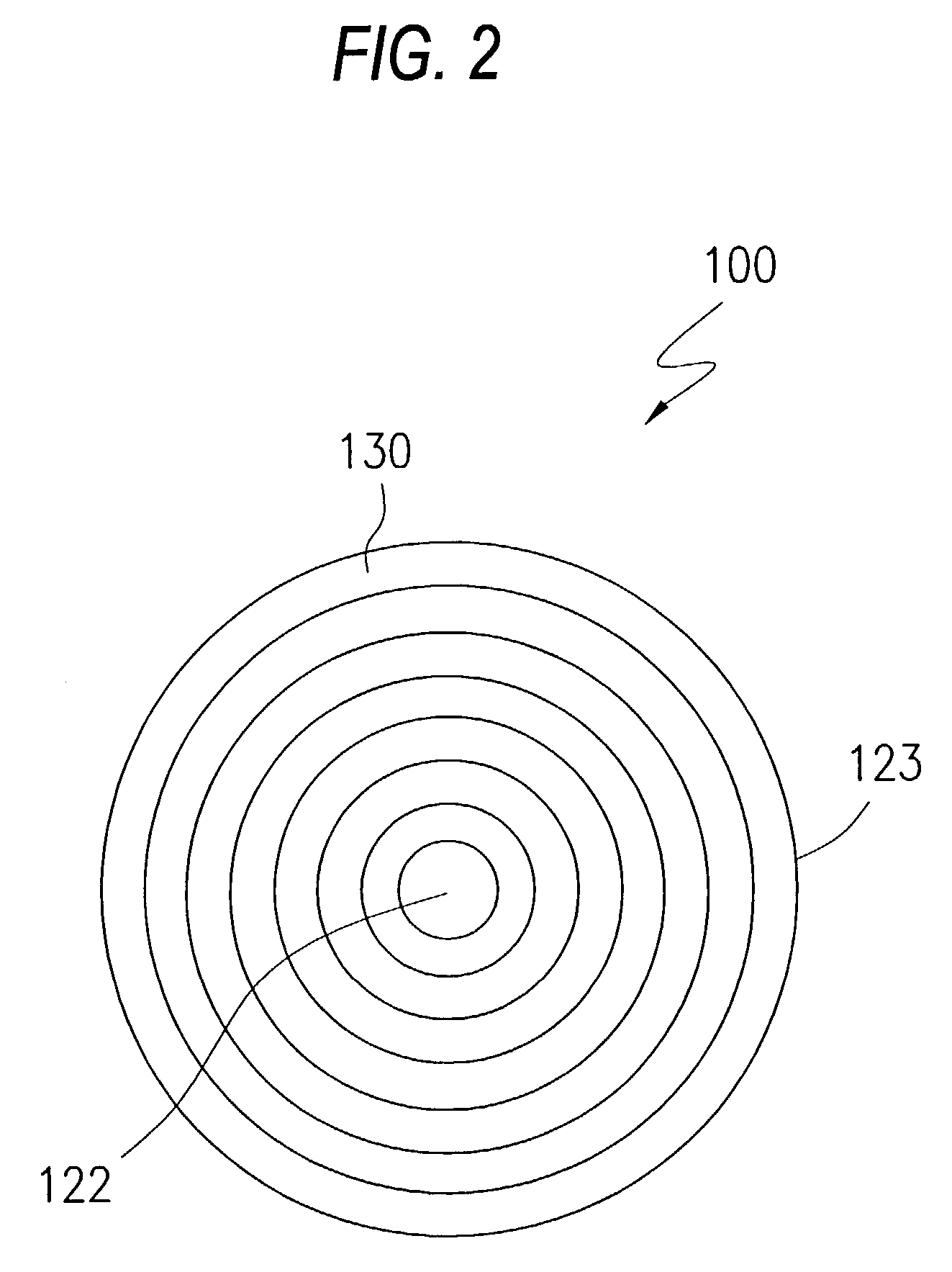
[0026]FIG. 1 is a partial cross-sectional view of a semiconductor wafer 100 having a substrate 110 and a metal layer 130 deposited on a low conductivity layer 120 in accordance with the present invention. The low conductivity layer 120 may be barrier layer, such a...


PUM

PropertyMeasurementUnit
Electric potential / voltageaaaaaaaaaa
Frequencyaaaaaaaaaa

Abstract

A method of electroplating metal onto a low conductivity layer combines a potential or current reversal waveform with variation in the amplitude and duration of the applied potential or current pulse. The method includes, over time, varying the duration of the pulse and continuously decreasing the amplitude of both the cathodic and anodic portions of the waveform across the surface of the low conductivity layer as the deposition zone moves from the center of the surface of the low conductivity layer to the outside edge. By virtue of the ability to vary the amplitude and duration of the pulse, the method facilitates the filling of structures in the center of the low conductivity layer without overdepositing on the outside edge, thus ensuring a controlled deposition of material across the surface of the low conductivity layer.

Description

[0001]This application is a divisional application of U.S. patent application Ser. No. 09 / 938,645, filed Aug. 27, 2001 now U.S. Pat. No. 6,723,219, the entirety of which is incorporated herein by reference.BACKGROUND OF THE INVENTION[0002]1. Field of the Invention[0003]This invention relates generally to the field of electroplating. The invention relates more specifically to a method of electroplating, and a layer of electroplated material deposited therewith, that are suitable for deposition on a low conductivity substrate material.[0004]2. Description of the Related Art[0005]Various difficulties are associated with the electroplating of metals such as copper onto low conductivity barrier materials such as Ta and W. In the context of semiconductor fabrication, the major problem associated with plating on such barriers is that of achieving the required adhesion and uniformity of the electroplated layer across the surface of a wafer without the presence of fill defects.[0006]Pulse pl...

Claims


Application Information

Patent Timeline
IPC IPC(8): C25D7/12C25D5/18C25D3/38H01L21/288H01L21/768
CPCC25D3/38C25D5/18C25D7/12H01L21/2885C25D17/001H01L21/76877Y10T428/12882Y10S205/92Y10T428/12528Y10T428/12819Y10T428/31678C25D7/123
Inventor COLLINS, DALE W.
Owner MICRON TECH INC
Why Eureka
Try Eureka