Semiconductor device for reducing the number of probing pad used during wafer test and method for testing the same

a technology of semiconductor devices and wafers, which is applied in the direction of electronic circuit testing, measurement devices, instruments, etc., can solve the problems of wasting a lot of time testing all of the integrated circuits on the wafer using a single test system, and achieve the effect of reducing the test tim

Active Publication Date: 2006-02-21
SK HYNIX INC
View PDF10 Cites 132 Cited by
  • Summary
  • Abstract
  • Description
  • Claims
  • Application Information

AI Technical Summary

Benefits of technology

[0008]Further, a reduction of the test time is provided by using a limited number of test channels for testing a wafer and using a test system to test a circuit having a number of pads greater than the test channel.

Problems solved by technology

Therefore, a lot of time is needed to test all of the integrated circuits on the wafer using a single test system.

Method used


Image

  • Semiconductor device for reducing the number of probing pad used during wafer test and method for testing the same
  • Semiconductor device for reducing the number of probing pad used during wafer test and method for testing the same
  • Semiconductor device for reducing the number of probing pad used during wafer test and method for testing the same

Examples


Embodiment Construction

[0025]Now the preferred embodiments will be described with reference to the accompanying drawings. Since preferred embodiments are provided for the purpose that the ordinary skilled in the art are able to understand the disclosure, they may be modified in various manners and the scope of this disclosure is not limited by the preferred embodiments described herein.

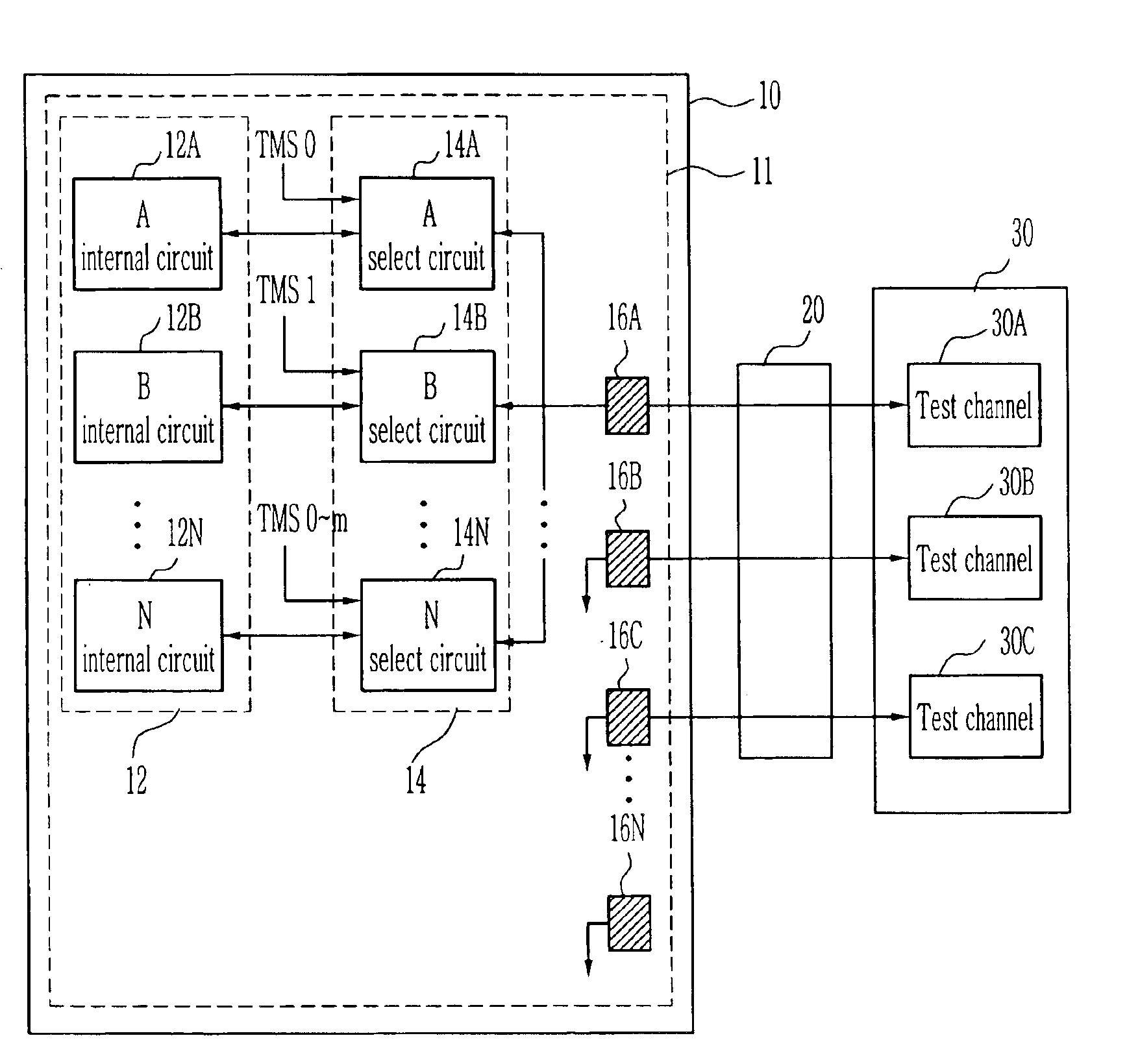
[0026]Referring to FIG. 1, the semiconductor device includes a select circuit unit 14 for testing a plurality of internal circuits 12A to 12N using a single probing pad 16A during wafer test. The select circuit unit 14 is synchronized to test mode signals (TMS0 to TMSm) during wafer test to transmit a test signal supplied from a test channel 30A of a test system 30 to the internal circuits 12A to 12N through the pad 16A. Further, the select circuit unit 14 selects one of output signals generated from the respective internal circuits 12A to 12N, in response to the test mode signal, to transmit the selected out signal to the ...


PUM


Abstract

The present invention relates to a semiconductor device and a method for testing the same capable of reducing the number of probing pads used during wafer test. The semiconductor device includes a select circuit connected between a plurality of internal circuits to be tested and a single probing pad, for transmitting test signals inputted from the probing pads to any one of the plurality of the internal circuits according to a test mode signal generated in a wafer test mode. It is possible to reduce the number of the probing pads in the integrated circuit used for connection to a probe for contact of a probe card during wafer test. It is therefore possible to reduce test time.

Description

BACKGROUND[0001]1. Technical Field[0002]A semiconductor device, a method for testing the same and a test system are disclosed that are capable of reducing the number of probing pads used during a wafer test.[0003]2. Discussion of Related Art[0004]Generally, integrated circuits of a semiconductor device are formed on a semiconductor wafer in the form of a die and then packaged. In order to avoid packaging defective integrated circuits, it is preferred to test the integrated circuits on each wafer. The testing of the integrated circuits include a series of transmitting a test signal to an input terminal, and then monitoring an output signal generated by the integrated circuit and outputted through an output terminal in order to decide whether the integrated circuit operates as expected.[0005]A typical integrated circuit test system includes ‘a test head’ having a circuit board for implementing a set of test channels. Each of the test channels includes the input channel for providing t...

Claims


Application Information

Patent Timeline
Patent Type & Authority Patents(United States)
IPC IPC(8): G01R31/28G11C29/00G01R31/317G01R31/3185
CPCG01R31/31715G01R31/318511G01R31/318505G01R31/3172G11C29/00
Inventor KANG, TAE JINLEE, WOON BOK
Owner SK HYNIX INC
Why Eureka
Try Eureka