Liquid crystal display driver integrated circuit package

a technology of integrated circuits and liquid crystal displays, which is applied in the direction of identification means, semiconductor/solid-state device details, instruments, etc., can solve the problems of affecting the displayed image, the limitation of the chip on the glass-type lcd device, etc., and achieves the effects of preventing deterioration of electric characteristics, reducing differences, and high quality of displayed images

Inactive Publication Date: 2006-02-21
SHENZHEN CHINA STAR OPTOELECTRONICS TECH CO LTD
View PDF1 Cites 17 Cited by
  • Summary
  • Abstract
  • Description
  • Claims
  • Application Information

AI Technical Summary

Benefits of technology

[0030]According to the present invention, there is provided decreased difference between the area of the bumps mounted at the signal lines for receiving an image signal and the area of the bumps mounted at the signal lines for outputting the driving signal. As a result of this decrease, deterioration of electric characteristics is prevented when the bumps and the signal lines are connected to the anisotropic conductive films and a high quality of the displayed images is maintained in an LCD.

Problems solved by technology

However, the chip on glass type LCD device also has limitations owing to characteristics of the chip on glass type LCD device.
This excessive or insufficient compression causes undesirable deteriorations in the electric characteristics, ultimately affecting the displayed image.

Method used


Image

  • Liquid crystal display driver integrated circuit package
  • Liquid crystal display driver integrated circuit package
  • Liquid crystal display driver integrated circuit package

Examples


Embodiment Construction

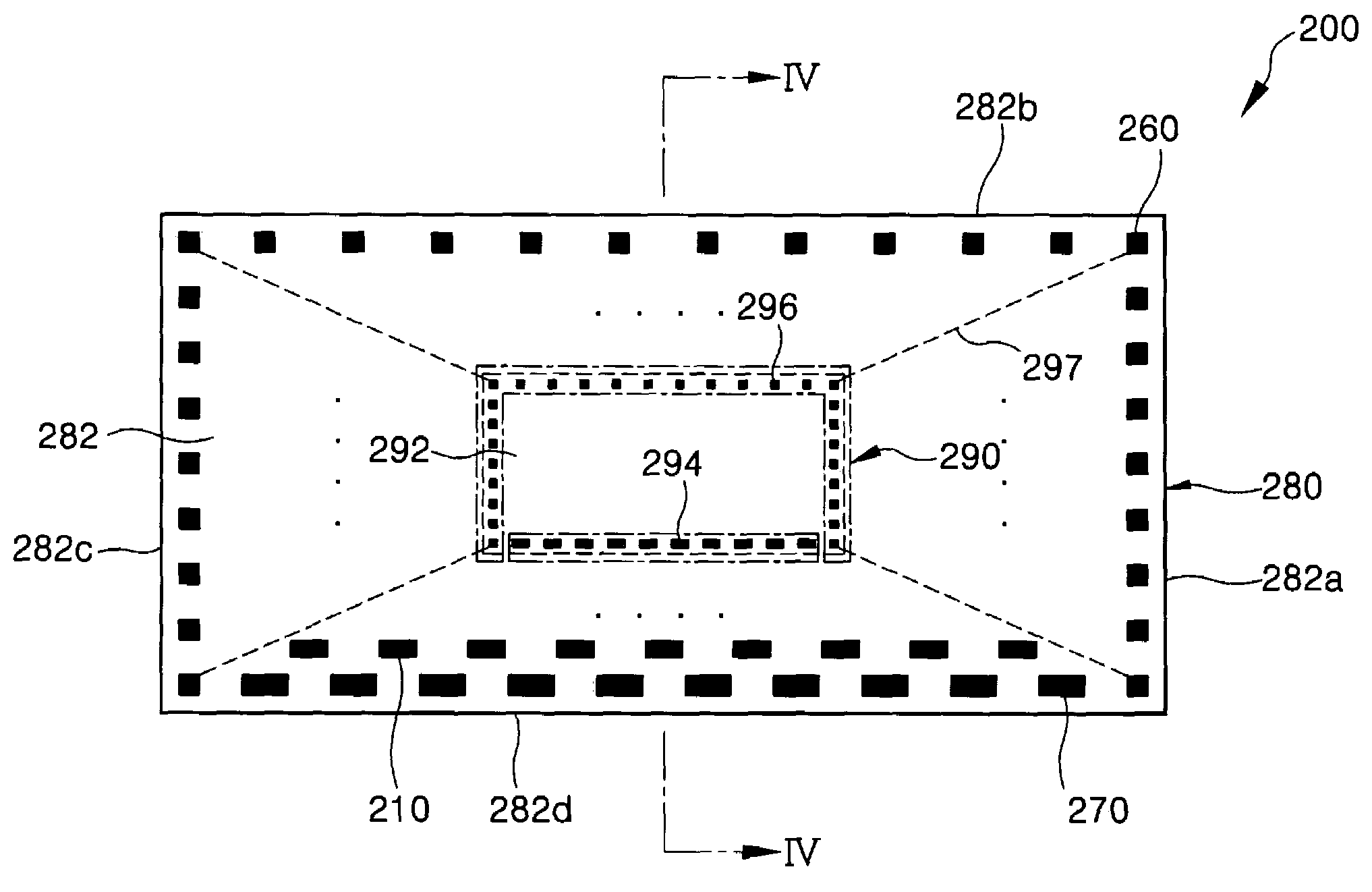
[0041]FIG. 3 is a schematic view showing an LCD driver integrated circuit package according to one exemplary embodiment of the present invention.

[0042]Referring to FIG. 3, a LCD driver integrated circuit package 200 includes a driving signal processing chip 290, a mold 280, driving signal output bumps 260, image signal input bumps 270 and bump pressure control patterns 210.

[0043]The driving signal processing chip 290 has a driving signal generating module 292, image signal input pads 294 and driving signal output pads 296. The driving signal generating module 292 processes an image signal from an external data processing device, and generates a driving signal for driving an LCD panel.

[0044]The image signal input pads 294 are formed on the driving signal generating module 292. A plurality of the image signal input pads 294 are arranged in a line at a portion of a surface of the driving signal generating module 292. The portion of the surface of the driving signal generating module 29...


PUM

PropertyMeasurementUnit
pressureaaaaaaaaaa
anisotropic conductiveaaaaaaaaaa
voltageaaaaaaaaaa

Abstract

Disclosed is an LCD driver integrated circuit package and a chip on glass type LCD device using the package. The LCD driver integrated circuit package includes a mold that has signal output bumps and signal input bumps formed thereon, wherein the signal output bumps and the signal input bumps have different surface areas that contact the mold and an adjacent conductive film. Due to the different contact surface areas, different amounts of pressure are applied to different parts on the conductive film when a force is applied to the mold. One or more bump pressure control patterns are formed on the mold compensate for the difference in pressure caused by this difference between the total contact areas. Accordingly, the LCD driver integrated circuit package can be mounted on a chip on glass type LCD panel without causing device failure.

Description

CROSS-REFERENCES TO RELATED APPLICATIONS[0001]This patent application claims priority from Korean Patent Application No. 2002-23768 filed on Apr. 30, 2002 under 35 U.S.C. §119 and incorporates this Korean patent application by reference herein in its entirety.BACKGROUND OF THE INVENTION[0002]1. Field of the Invention[0003]The disclosure relates to a liquid crystal display (LCD) driver integrated circuit package and a chip on glass type LCD device using the same, and more particularly to an LCD driver integrated circuit package and a chip on glass type LCD device capable of decreasing bonding failures that occur during a mounting process for an LCD device.[0004]2. Description of the Prior Art[0005]Generally, an LCD device is a flat panel display device for displaying characters, images and motion pictures by means of liquid crystal.[0006]The LCD device includes an LCD panel for controlling the image that is generated, a light supplying device for providing light to the LCD and a driv...

Claims


Application Information

Patent Timeline
Patent Type & Authority Patents(United States)
IPC IPC(8): H01R12/16G02F1/1345G02F1/13G09F9/00H01L23/28
CPCG02F1/13452H01L24/06H01L2224/0603H01L2224/05554H01L2224/05553H01L2224/49171H01L2924/181H01L2924/14H01L2924/00G02F1/1345
Inventor LEE, SUNG-HO
Owner SHENZHEN CHINA STAR OPTOELECTRONICS TECH CO LTD
Why Eureka
Try Eureka