Check patentability & draft patents in minutes with Patsnap Eureka AI!

Memory bus interface for use in a peripheral device

a technology of memory bus and peripheral device, applied in the field of computer systems, can solve problems such as latency and arbitration problems of the communication mechanism

Active Publication Date: 2006-02-21
MICROCHIP TECH INC
View PDF10 Cites 10 Cited by
  • Summary
  • Abstract
  • Description
  • Claims
  • Application Information

AI Technical Summary

Benefits of technology

The patent describes systems and methods for interfacing a peripheral device to a memory bus. The interface includes a memory bus interface and a device interface that can communicate data to and from the peripheral device. The interface can support different memory protocols and can participate in burst transfers of data on the memory bus. The peripheral device can perform various functions such as data communication, video functions, printing functions, mass storage, and human interface controller functions. The technical effect of the patent is to provide a flexible and efficient way to connect peripheral devices to a memory bus and to perform various functions on data accessed by the peripheral device.

Problems solved by technology

This mechanism for communicating may experience latency and arbitration problems due to the presence of other devices 36 on the PCI bus 30.

Method used


Image

  • Memory bus interface for use in a peripheral device
  • Memory bus interface for use in a peripheral device
  • Memory bus interface for use in a peripheral device

Examples


Embodiment Construction

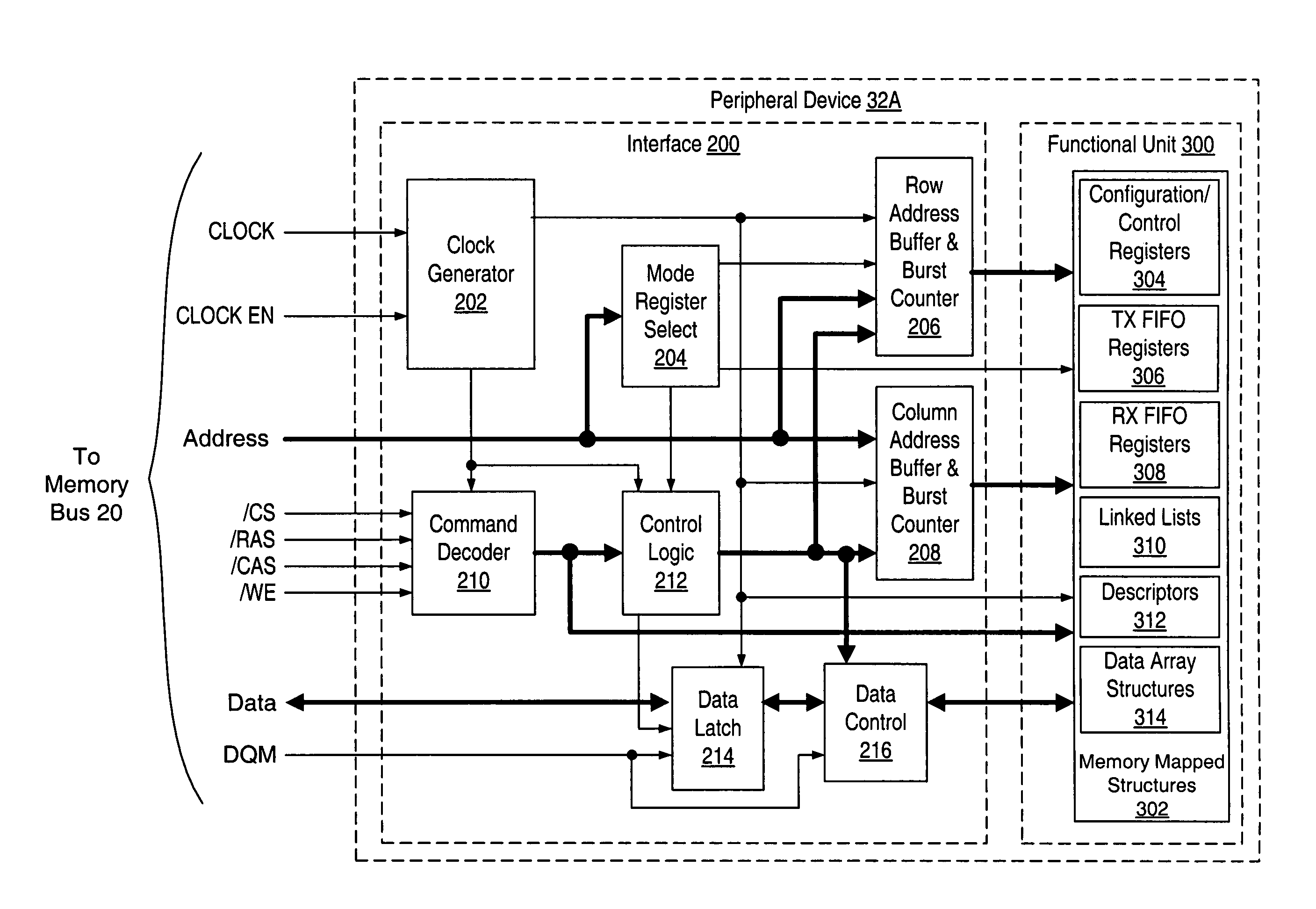
[0020]FIG. 2 illustrates a block diagram of a computer system 100 that includes a peripheral device 32A configured to interface to a memory bus 20, according to one embodiment. In FIG. 2, an embedded controller 12 is coupled to a memory bus 20 and a PCI bus 30. Embedded controller 12 includes a processor 14, a memory system controller 16, and an I / O system controller 18. Memory bus 20 is coupled to two memory modules 22A and 22B and a peripheral device 32A. PCI bus 30 is coupled to a PCI device 36. PCI bus 36 is illustrated as an exemplary peripheral or I / O bus. Other peripheral bus technologies such as ISA (Industry Standard Architecture) and USB (Universal Serial Bus) may be used in other embodiments.

[0021]In some embodiments, the memory system controller 16 may be configured to transmit standard SDRAM (Synchronous Dynamic Random Access Memory) control and address signals to SDRAM memory modules 22A and 22B via memory bus 20. In one such embodiment, memory modules 22A and 22B may ...


PUM


Abstract

A peripheral device may include an interface configured to interface to a memory bus and a functional unit coupled to the interface and configured to perform a peripheral device function on data accessed by the interface. The interface may be configured to perform a data access in response to memory control, address, and data signals on the memory bus. The functional unit may be configured to perform various peripheral device functions such as data communication functions, video functions, printing functions, mass storage functions, and human interface controller functions.

Description

FIELD OF THE INVENTION[0001]This invention relates to computer systems and, more particularly, to transferring data to a peripheral device within a computer system.DESCRIPTION OF THE RELATED ART[0002]FIG. 1 illustrates a typical configuration of a computer system 10 that includes an embedded controller 12, several memory modules 22A–22B, a memory bus 20, a PCI (Peripheral Component Interconnect) bus 30, an Ethernet MAC (Media Access Control) 32 and associated PHY (PHYsical Layer) device 34, and another PCI device 36. The embedded controller 12 includes a processor 14 and a bus bridge that includes a memory system controller 16 and an I / O system controller 18. The memory controller 16 allows the processor to communicate with memory modules 22A–22B via transfers over memory bus 20. I / O system controller 18 allows the processor 14 to communicate with the Ethernet MAC 34 and PCI device 36 via the PCI bus 30.[0003]When the data is being transferred to or from computer system 100 via the ...

Claims


Application Information

Patent Timeline
Patent Type & Authority Patents(United States)
IPC IPC(8): G06F12/00G06F13/40
CPCG06F13/404
Inventor BRANT, PAUL M.STONE, III, JOHN E.
Owner MICROCHIP TECH INC
Features
  • R&D
  • Intellectual Property
  • Life Sciences
  • Materials
  • Tech Scout
  • Unparalleled Data Quality
  • Higher Quality Content
  • 60% Fewer Hallucinations
Learn More