Bump forming apparatus for charge appearance semiconductor substrate, charge removal method for charge appearance semiconductor substrate, charge removing unit for charge appearance semiconductor substrate, and charge appearance semiconductor substrate

a technology of semiconductor substrate and forming apparatus, which is applied in the direction of electrical equipment, basic electric elements, semiconductor devices, etc., can solve the problems of increased process and cost, unfavorable cycle time, and ultrasonic vibration, so as to reduce the amount of charge, prevent the breakage of the substrate itself, and eliminate the charge generated on the substrate

Inactive Publication Date: 2006-02-28
PANASONIC CORP
View PDF20 Cites 3 Cited by
  • Summary
  • Abstract
  • Description
  • Claims
  • Application Information

AI Technical Summary

Benefits of technology

[0038]A charge removal method according to a 15th aspect of the present invention, comprises bringing a charge appearance semiconductor substrate defined in the 14th aspect into contact with a contact member for charge removal defined in the ninth aspect; and eliminating charge generated on the substrate.
[0039]According to the charge appearance semiconductor substrate of the 14th aspect and the charge removal method of the 15th aspect, the region for charge removal and the dicing lines are arranged so that charge generated on the charge appearance semiconductor substrate can be eliminated from the region for charge removal, or via the region for charge removal and the dicing lines. The damage resulting from the charge such as pyroelectric breakdown of the circuit formed on the substrate and breakage of the substrate itself can be prevented accordingly. An amount of charge of the charge appearance semiconductor substrate varies, for example, depending on the manner of earthing from the circuit-formed parts of the substrate to the dicing lines of the substrate. The amount of charge can be reduced to approximately ±20V without using the ion generator when electric charge is removed most effectively. The amount of charge can be reduced to approximately ±200V on average.
[0040]According to a 16th aspect of the present invention, a charge appearance semiconductor substrate has an amount of charge of not larger than ±200V because of eliminating charge generated on the charge appearance semiconductor substrate which generates charge due to a temperature change.

Problems solved by technology

But the aluminum film of the rear face may be separated to cause troubles at the application of a pressure and ultrasonic vibration to the rear face by a pressing member because the pressure and ultrasonic vibration are applied with the pressing member brought into contact with the rear face, for example, when each chip cut out from the wafer is flip chip mounted to the substrate via the bump.
Therefore, the aluminum film formed for the purpose of elimination of charge should be removed before the chip is mounted, resulting in an increase of processes and costs.
As a result, a cycle time becomes undesirably lengthy in the case of the piezoelectric substrate 11, as compared with conventional silicon wafers not accompanied with generation of charge.

Method used


Image

  • Bump forming apparatus for charge appearance semiconductor substrate, charge removal method for charge appearance semiconductor substrate, charge removing unit for charge appearance semiconductor substrate, and charge appearance semiconductor substrate
  • Bump forming apparatus for charge appearance semiconductor substrate, charge removal method for charge appearance semiconductor substrate, charge removing unit for charge appearance semiconductor substrate, and charge appearance semiconductor substrate
  • Bump forming apparatus for charge appearance semiconductor substrate, charge removal method for charge appearance semiconductor substrate, charge removing unit for charge appearance semiconductor substrate, and charge appearance semiconductor substrate

Examples


Embodiment Construction

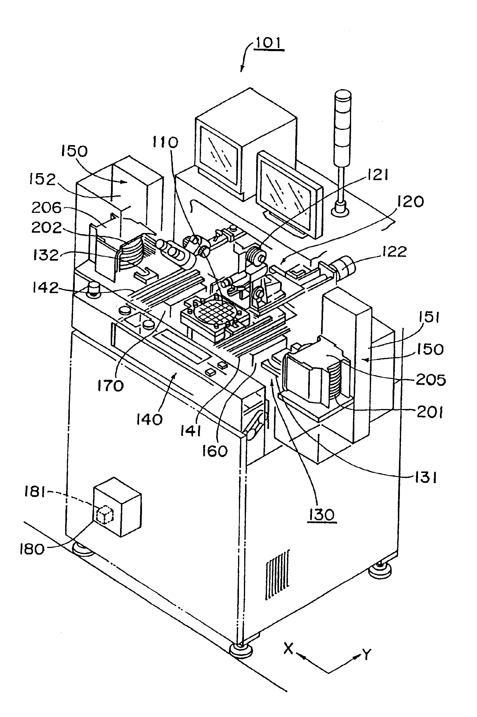
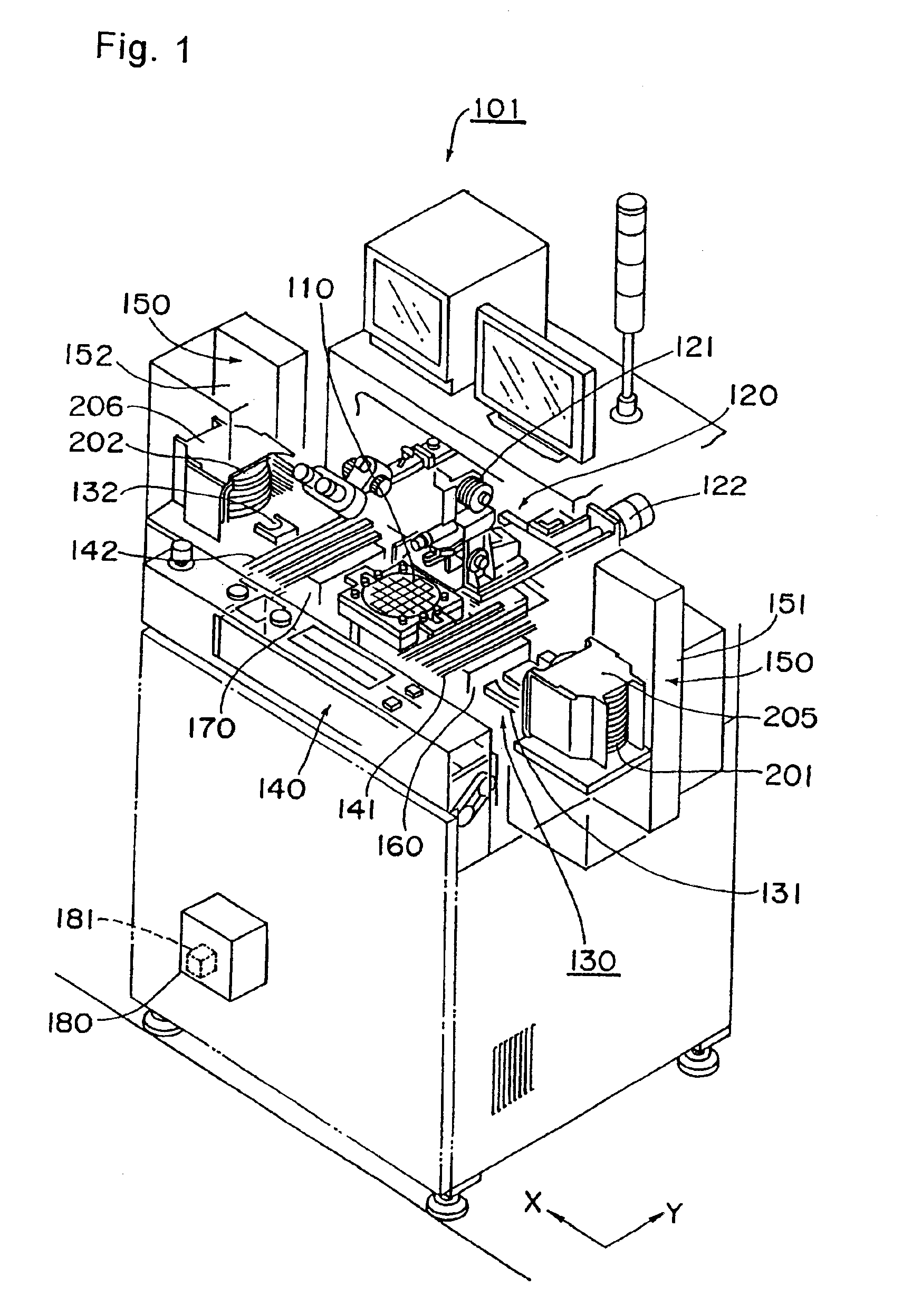
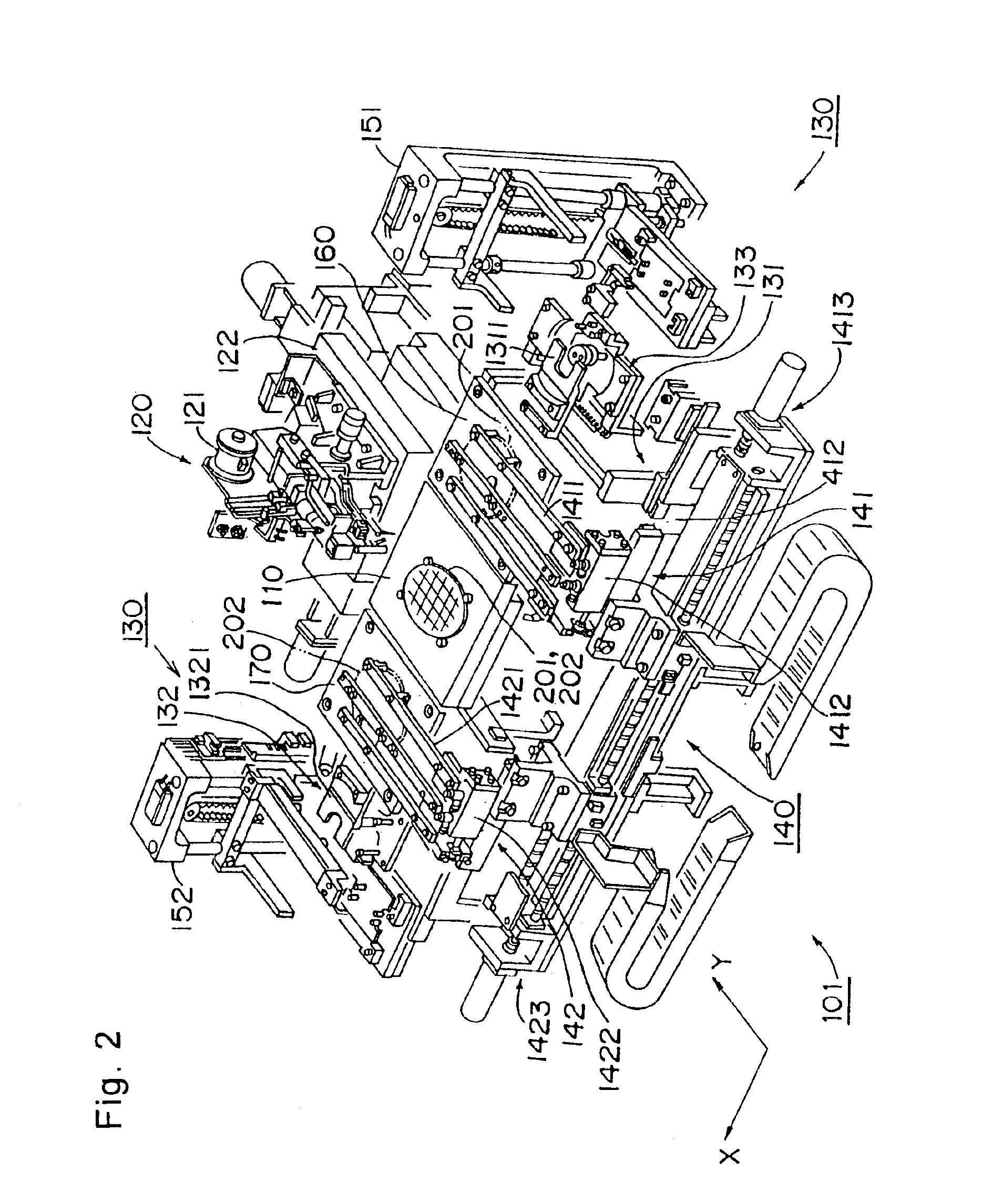
[0139]A bump forming apparatus, a method carried out by the bump forming apparatus for removing charge from a charge appearance semiconductor substrates, a charge removing unit installed on the bump forming apparatus for removing charge of the charge appearance semiconductor substrates, and a charge appearance semiconductor substrate which are embodiments of the present invention will be described with reference to the drawings. It is to be noted that like parts are designated by like reference numerals throughout the drawings.

[0140]A bump forming apparatus 101 according to the embodiment shown in FIGS. 1 and 2 is appropriate to process a wafer-shaped piezoelectric substrate (referred to as a “piezoelectric substrate wafer” hereinafter) for forming the SAW filter mentioned before, and will be described below by way of example to form bumps to the piezoelectric substrate wafer. However, objects to be processed by the apparatus are not limited to the piezoelectric substrate wafer. In ...


PUM


Abstract

The present invention provides a bump forming apparatus (101, 501) which can prevent charge appearance semiconductor substrates (201, 202) from pyroelectric breakdown and physical failures, a method carried out by the bump forming apparatus for removing charge of charge appearance semiconductor substrates, a charge removing unit for charge appearance semiconductor substrates, and a charge appearance semiconductor substrate. At least when the wafer is cooled after the bump bonding is connected on the wafer, electric charge accumulated on the wafer (202) because of the cooling is removed through direct contact with a post-forming bumps heating device (170), or the charge is removed by a decrease in temperature control so that charge can be removed in a noncontact state. Therefore, an amount of charge of the wafer can be reduced in comparison with the conventional art, so that the wafer is prevented from pyroelectric breakdown and damage such as a break or the like to the wafer itself.

Description

[0001]This is a Divisional Application of U.S. application Ser. No. 10 / 019,700, filed Jan. 2, 2002, now U.S. Pat. No. 6,818,975 which is the National Stage of International Application No. PCT / JP00 / 04280, filed Jun. 29, 2000.TECHNICAL FIELD[0002]The present invention relates to a bump forming apparatus for forming bumps onto a charge appearance type semiconductor substrate such as a piezoelectric substrate or the like which generate electric charge in accordance with a temperature (that is, a charge appearance semiconductor substrate), a method carried out by the bump forming apparatus for removing charge of the charge appearance semiconductor substrate, a charge removing unit installed in the bump forming apparatus for charge appearance semiconductor substrates, and a charge appearance semiconductor substrate.BACKGROUND ART[0003]Electronic components installed in devices, e.g., portable phones and the like have been made compact these days in association with a great miniaturizatio...

Claims


Application Information

Patent Timeline
Patent Type & Authority Patents(United States)
IPC IPC(8): H01L21/44H01L21/00
CPCH01L21/67138H01L21/67144Y10S438/974H01L21/60
Inventor NARITA, SHORIKITSUBOI, YASUTAKAIKEYA, MASAHIKOMAE, TAKAHARUKANAYAMA, SHINJI
Owner PANASONIC CORP
Why Eureka
Try Eureka