Dual metal gate process: metals and their silicides

a metal gate and metal silicide technology, applied in the direction of solid-state devices, electric devices, transistors, etc., can solve the problems of buried channel effects, threshold voltage becomes too high for both types of transistors, and single metal gate work function values that are not suitable for cmos applications, etc., to achieve work functions. the effect of higher or lower work functions

Inactive Publication Date: 2006-02-28
CHARTERED SEMICONDUCTOR MANUFACTURING
View PDF8 Cites 24 Cited by
  • Summary
  • Abstract
  • Description
  • Claims
  • Application Information

AI Technical Summary

Benefits of technology

[0013]In accordance with the objects of the invention, a method for forming dual-metal gate CMOS transistors is achieved. First and second active areas of a semiconductor substrate are separated by isolation regions. One of the active areas will be PMOS and the other will be NMOS. A gate dielectric layer is formed overlying the semiconductor substrate in each of the active areas. A metal layer is deposited overlying the gate dielectric layer. Silicon ions are implanted into the metal layer in the PMOS area to form an implanted metal layer and the implanted metal layer is silicided to form a metal silicide layer. Thereafter, the metal layer and the metal silicide layer are patterned to form a metal gate in a first active area and a metal silicide gate in a second active area to complete formation of dual-metal gate CMOS transistors in the fabrication of an integrated circuit. The metal silicide may have a higher or lower work function depending on the metal used. The PMOS gate will be formed from the gate having the higher work function.

Problems solved by technology

It is anticipated that a single metal gate with mid-gap work function values will not be suitable for CMOS applications due to buried channel effects.
By using a single metal gate for both NMOSFET and PMOSFET, the threshold voltage becomes too high for both types of transistors.
In order to achieve a lower threshold voltage, additional implantation is required and this will result in buried channel effects.

Method used


Image

  • Dual metal gate process: metals and their silicides
  • Dual metal gate process: metals and their silicides
  • Dual metal gate process: metals and their silicides

Examples


Embodiment Construction

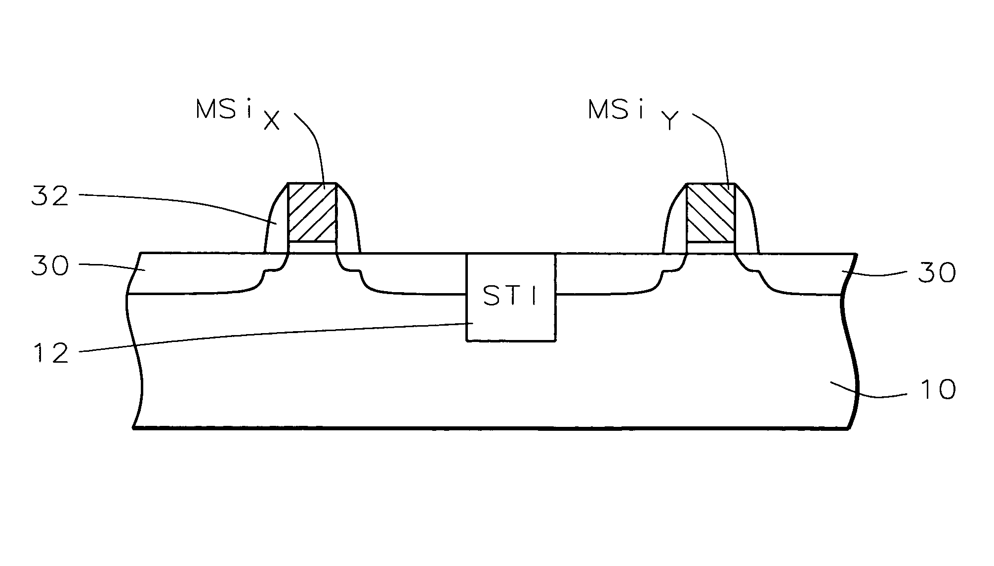
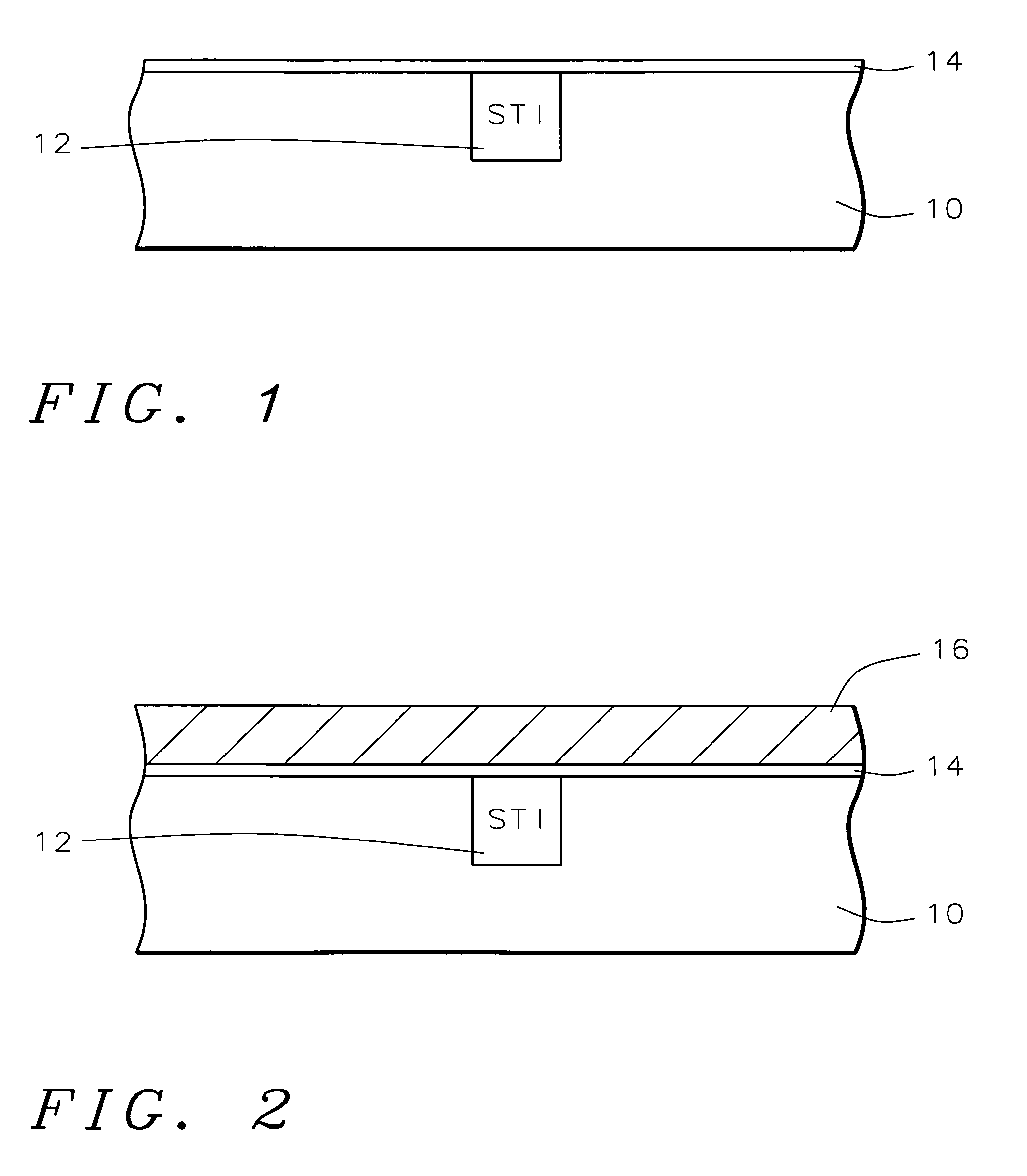
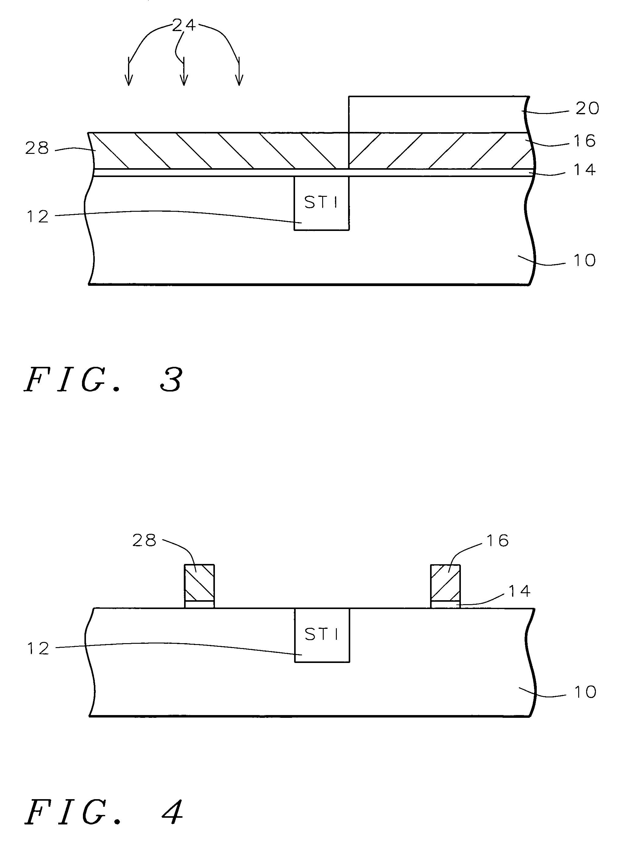
[0023]The present invention uses a metal and its metal silicide to form dual-metal gates having different work functions. In one embodiment, two different silicides of the metal are used as the dual-metal gates. It will be understood by those skilled in the art that the invention should not be limited to the embodiments described herein, but can be extended and applied to any application in which it is desired to have metal gates having differing work functions. The first embodiment of the invention will be described with reference to FIGS. 1–5. The second embodiment of the invention will be described with reference to FIGS. 6–11. The third embodiment of the invention will be described with reference to FIGS. 12 and 13.

[0024]Referring now to FIGS. 1–5, the first preferred embodiment of the present invention will be described. Referring now more particularly to FIG. 1, there is shown a semiconductor substrate 10. This is preferably monocrystalline silicon. Isolation regions, such as ...


PUM

PropertyMeasurementUnit
thicknessaaaaaaaaaa
thicknessaaaaaaaaaa
thicknessaaaaaaaaaa

Abstract

Methods for forming dual-metal gate CMOS transistors are described. An NMOS and a PMOS active area of a semiconductor substrate are separated by isolation regions. A metal layer is deposited over a gate dielectric layer in each active area. Silicon ions are implanted into the metal layer in one active area to form an implanted metal layer which is silicided to form a metal silicide layer. Thereafter, the metal layer and the metal silicide layer are patterned to form a metal gate in one active area and a metal silicide gate in the other active area wherein the active area having the gate with the higher work function is the PMOS active area. Alternatively, both gates may be metal silicide gates wherein the silicon concentrations of the two gates differ. Alternatively, a dummy gate may be formed in each of the active areas and covered with a dielectric layer. The dielectric layer is planarized thereby exposing the dummy gates. The dummy gates are removed leaving gate openings to the semiconductor substrate. A metal layer is deposited over a gate dielectric layer within the gate openings to form metal gates. One or both of the gates are silicon implanted and silicided. The PMOS gate has the higher work function.

Description

RELATED PATENT APPLICATION[0001]This is a division of patent application Ser. No. 10 / 266,714, filing date Oct. 8, 2002, now U.S. Pat. No. 6,750,519, A Dual Metal Gate Process: Metals And Their Silicides, which is divison of patent application Ser. No. 09 / 981,415, filing date Oct. 18, 2001, now U.S. Pat. No. 6,475,908, A Dual Metal Gate Process: Metals And Their Silicides, assigned to the same assignee as the present invention, which are herein incorporated by reference in their entirety.[0002]U.S. patent application Ser. No. 09 / 981,416 to the same inventors, filed on Oct. 18, 2001.BACKGROUND OF THE INVENTION[0003](1) Field of the Invention[0004]The present invention relates to the fabrication of integrated circuit devices, and more particularly, to a method of fabricating dual-metal transistors having different work functions in the fabrication of integrated circuits.[0005](2) Description of the Prior Art[0006]It is anticipated that a single metal gate with mid-gap work function val...

Claims


Application Information

Patent Timeline
Patent Type & Authority Patents(United States)
IPC IPC(8): H01L29/76H01L29/94H01L31/062H01L31/113H01L31/119H01L21/28H01L21/336H01L21/8238
CPCH01L21/28097H01L21/823835H01L29/66545H01L21/823842H01L29/517
Inventor LIN, WENHEZHOU, MEI-SHENGPEY, KIN LEONGCHOOI, SIMON
Owner CHARTERED SEMICONDUCTOR MANUFACTURING
Why Eureka
Try Eureka