

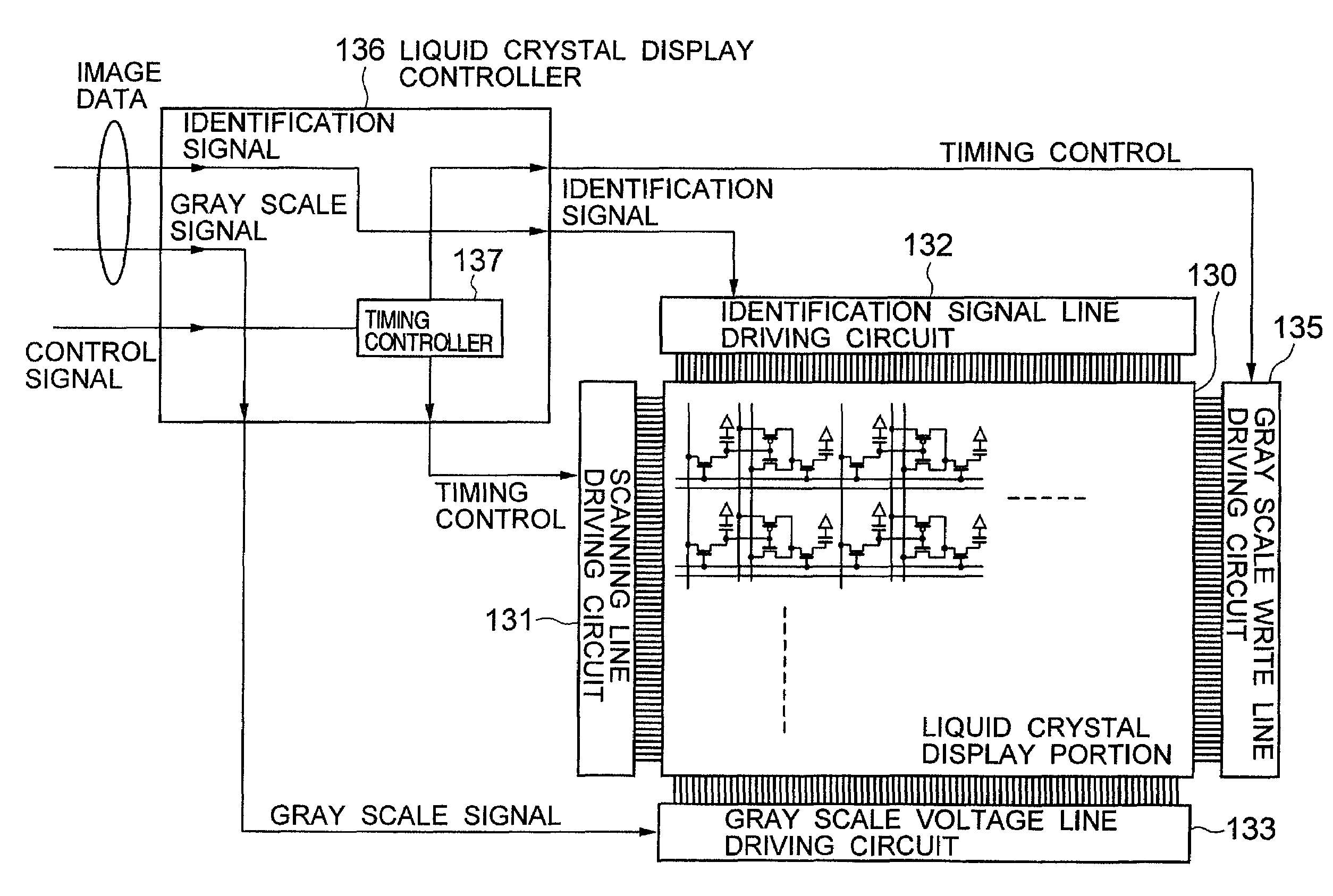
Display apparatus with pixels arranged in matrix
a display apparatus and matrix technology, applied in the field of display apparatuses, can solve the problems of insufficient security of the line sequential driving system, failure to normally display images, and delay in the liquid crystal driving voltage supplied to the pixel capacitance, so as to improve the processing capacity of the data processing circuit, and display a greater quantity of information
- Summary
- Abstract
- Description
- Claims
- Application Information
AI Technical Summary
Benefits of technology
Problems solved by technology
Method used
Image

Examples
embodiment 1
[0043]Referring initially to FIG. 3, an image data format that a display apparatus according to the present invention receives will be explained.
[0044]Image data is generally expressed as a group of pixels having gray scale data for each color. In the image format widely used in PC (personal computer), for example, each pixel data is separated into the three primary colors of red (R), green (G) and blue (B), and is described as data of 8 bits=256 gray scales from lightness to darkness for each color. The image information quantity of one pixel is in this case 8 bits×3 (colors)=24 bits. One screen image data as a group of these pixel data is referred to as a “bit map”. In an image output source of PC or the like, a memory stores this bit map. A conventional image outputting method outputs the data from the upper left part to the lower right part of the bit map in a dot sequential driving system. On the other hand, the display apparatus receives the data outputted in the dot sequentia...
embodiment 2
[0059]Next, Embodiment 2 will be explained. FIG. 5 shows a pixel circuit diagram of the display apparatus of this embodiment. This embodiment is different from Embodiment 1 in the construction of the light modulator 112. Namely, the light modulator 112 of this embodiment comprises an LED light modulator including a holding capacitance 113, a fifth active device 115 using the pixel electrode 111 as its gate terminal and an LED device 116 connected to a current source through the fifth active device 115. The construction of this embodiment other than the light modulator 112 is the same as that of Embodiment 1.
[0060]The gray scale voltage written to the pixel electrode 111 is simultaneously written to the holding capacitance 113, too. This voltage drives the fifth active device 115 and controls the current flowing through the LED (Light Emitting Diode) device 116 to thereby modulate a light emission quantity. When the LED light modulator is used as the light modulator 112 in this way, ...
embodiment 3
[0062]Next, Embodiment 3 will be explained. FIG. 6 shows a pixel circuit diagram of the display apparatus of this embodiment. In Embodiment 1, the gray scale voltage lines (1 and 2) are connected to each pixel. In this embodiment, however, mutually adjacent pixels share the gray scale voltage lines, and the display apparatus is functionally and substantially equivalent. The only limitation is that one block can be constituted by only (2n pixels in the transverse direction)×(n′ pixels in the vertical direction) though one block can be constituted by n×n′ pixels (n and n′: arbitrary numbers) in Embodiment 1. In practice, however, the number of pixels in both longitudinal and transverse directions of one block is even-numbered in most cases, and this limitation hardly becomes a problem.
[0063]Since this embodiment can decrease the number of lead wires per pixel, short-circuit among the lead wires can be reduced during production and the yield can be improved. In consequence, the display...
PUM
| Property | Measurement | Unit |
|---|---|---|
| voltage | aaaaa | aaaaa |
| gray scale voltage | aaaaa | aaaaa |
| capacitance | aaaaa | aaaaa |
Abstract
Description
Claims
Application Information