Self timed bit and read/write pulse stretchers

a self-timed bit and pulse stretcher technology, applied in static storage, information storage, digital storage, etc., can solve the problems of unsatisfactory and unreliable write, unreliable write, and inability to read/write, so as to improve the reliability of ram data

Active Publication Date: 2006-02-28
TWITTER INC
View PDF7 Cites 8 Cited by
  • Summary
  • Abstract
  • Description
  • Claims
  • Application Information

AI Technical Summary

Benefits of technology

[0010]It is a purpose of the invention to improve RAM data reliability;
[0011]It is another purpose of the invention to minimize RAM write access time;
[0012]It is yet another purpose of the invention to insure data is written reliably to selected cells in a minimized write access time.

Problems solved by technology

If insufficient signal develops (i.e., <δ) in the cell, however, the data write may fail and, the cell may remain unswitched or become meta-stable.
Either result is unsatisfactory and unreliable because cell contents are indeterminate.
So, the write may fail, for example, if the word line drops too soon or, the bit line pair voltage change too soon, e.g., from the write driver terminating prematurely.
Unfortunately, once sufficient additional time is added for restoring the bit lines and write driver, access cycles are considerably longer than the word line select, perhaps as much as three or four times as long.
This impairs SRAM performance and performance for anything accessing the SRAM.

Method used


Image

  • Self timed bit and read/write pulse stretchers
  • Self timed bit and read/write pulse stretchers
  • Self timed bit and read/write pulse stretchers

Examples


Embodiment Construction

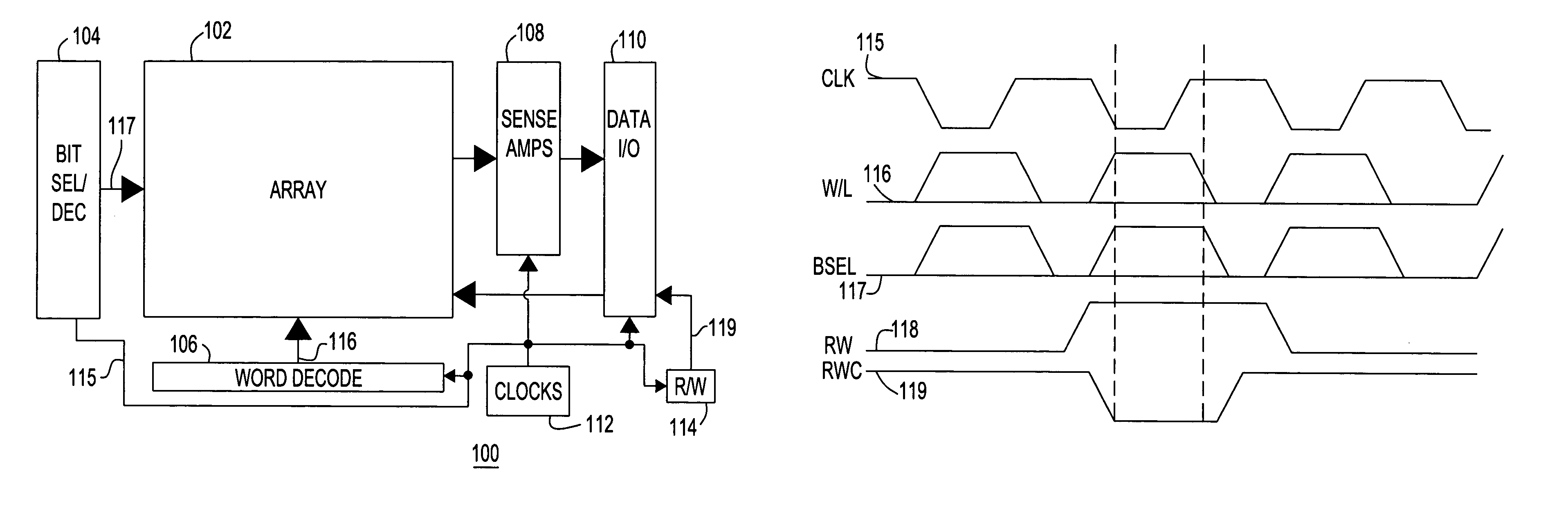
[0021]Referring now to the drawings, and more particularly, FIG. 1A shows an example of a block diagram of a memory 100, e.g., a random access memory (RAM) macro or chip, with a high performance self timed bit decode and write pulse stretcher, according to a preferred embodiment of the present invention. FIG. 1B shows a timing diagram for the memory example of FIG. 1A. In this example, the memory array 102 includes cells of well known six transistor (6T) latches or storage cells or 8T 2 port RAM cells (not shown) organized in N rows of word lines by M columns of K bit lines. More particularly, the storage array may be a typical CMOS SRAM or 2 port SRAM in what is known as silicon on insulator (SOI) technology, although application of the present invention is advantageous to almost any technology and any SRAM.

[0022]Cell selection is by coincidence a column selected by preferred bit decode and select circuit 104 with a row selected by word decoder 106. Selected cells are coupled to su...


PUM


Abstract

Bit and write decode / drivers, a random access memory (RAM) including the decode / drivers and an IC with a static RAM (SRAM) including the decode / drivers. The decode / drivers are clocked by a local clock and each produce access pulses wider than corresponding clock pulses. The bit decode / driver produces bit select pulses that are wider than a word select pulse and the write decode / driver produces write pulses that are wider than the bit select pulses for stable self timed RAM write accesses.

Description

BACKGROUND OF THE INVENTION[0001]1. Field of the Invention[0002]The present invention is related to random access memories (RAMs) and more particularly to static RAM (SRAM) access timing.[0003]2. Background Description[0004]Integrated circuits (ICs) are commonly made in the well-known complementary insulated gate field effect transistor (FET) technology known as CMOS. A typical CMOS circuit includes paired complementary devices, i.e., an n-type FET (NFET) paired with a corresponding p-type FET (PFET), usually gated by the same signal. Since the pair of devices have operating characteristics that are, essentially, opposite each other, when one device (e.g., the NFET) is on and conducting (ideally modeled as a closed switch), the other device (the PFET) is off, not conducting (ideally modeled as an open switch) and, vice versa. For example, a CMOS inverter is a series connected PFET and NFET pair that are connected between a power supply voltage (Vdd) and ground (GND).[0005]A typical ...

Claims


Application Information

Patent Timeline
Patent Type & Authority Patents(United States)
IPC IPC(8): G11C7/22G11C11/413G11C8/10G11C8/18G11C8/00G11C11/419
CPCG11C7/22G11C7/222G11C11/419G11C2207/229G11C2207/2281
Inventor JOSHI, RAJIV V.TUMINARO, ARTHUR D.
Owner TWITTER INC
Why Eureka
Try Eureka