Guard ring structure and method for fabricating same

a technology of guard rings and guard rings, which is applied in the direction of transistors, semiconductor devices, electrical equipment, etc., can solve the problems of device failure below the intrinsic limit of a discrete jfet, and process and geometries of guard rings used for bipolar devices are not fully compatible with the process and structures used for jfets and mesfets, so as to optimize the device breakdown characteristics

Inactive Publication Date: 2006-03-07
POWER INTEGRATIONS INC
View PDF9 Cites 33 Cited by
  • Summary
  • Abstract
  • Description
  • Claims
  • Application Information

AI Technical Summary

Benefits of technology

[0016]Accordingly, the present invention provides a guard ring structure that is applicable to JFETs and MESFETs, and is compatible with the processes used for fabrication of JFETs ...

Problems solved by technology

However, the supply voltage between the drain and source (Vds) is usually relatively low when the device is turned on.
However, when a JFET is integrated into another circuit, breakdown paths may be introduced that result in device failure below the intrinsic limit...

Method used


Image

  • Guard ring structure and method for fabricating same
  • Guard ring structure and method for fabricating same
  • Guard ring structure and method for fabricating same

Examples


Embodiment Construction

[0026]In the following detailed description of the present invention, a guard ring structure and a method for fabricating the structure, numerous specific details are set forth in order to provide a thorough understanding of the present invention. However, it will be obvious to one skilled in the art that the present invention may be practiced without these specific details. In other instances well known methods involving photolithography, deposition and etch, etc., and well known structures such as ohmic contacts and barrier metallization, etc., have not been described in detail so as not to unnecessarily obscure aspects of the present invention.

[0027]U.S. Pat. No. 6,251,716 entitled “JFET Structure and Manufacture Method for Low On-Resistance and Low Voltage Application,” issued Jun. 26, 2001, and assigned to the assignee of the present invention, is hereby incorporated herein by reference.

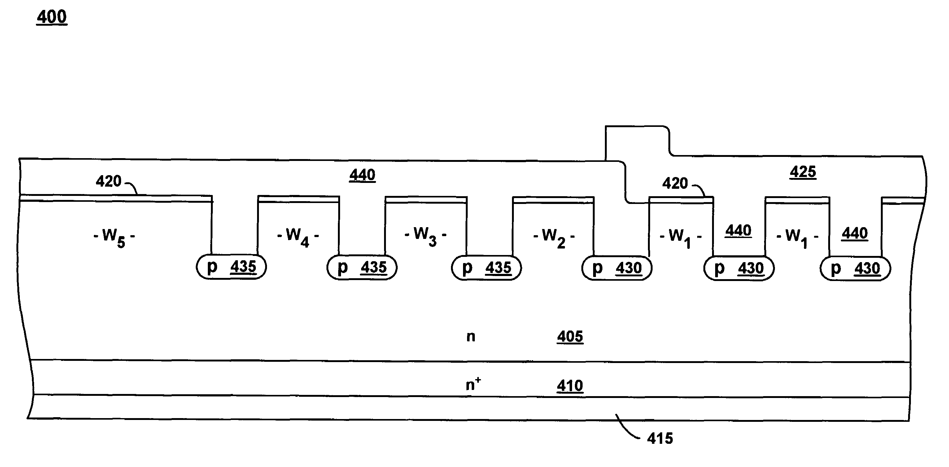
[0028]FIG. 4 shows a cross-section of an n-channel JFET 400 with a floating guard ring struc...


PUM


Abstract

A method for fabricating a guard ring structure for JFETs and MESFETs. Trenches are etched in a semiconductor substrate for fabrication of a gate structure for a JFET or MESFET. At time the gate trenches are etched, concentric guard ring trenches are also etched. The process used to fabricate the gate p-h junction or Schottky barrier at the bottom of the gate trenches is also used to fabricate the guard ring at bottom of the guard ring trenches. The separation between the guard ring trenches is 1.0 to 3.0 times greater than the separation between the gate trenches.

Description

FIELD OF THE INVENTION[0001]Embodiments of the present invention relate to field effect transistors (FETs). In particular, embodiments of the present invention relate to a guard ring structure for improved breakdown characteristics in FETs.BACKGROUND ART[0002]Junction field effect transistors (JFETs) are majority carrier devices that conduct current through a channel that is controlled by the application of a voltage to a p-n junction. JFETs may be constructed as p-channel or n-channel and may be operated as enhancement mode devices or depletion mode devices. Similar to the JFET is the metal-semiconductor field effect transistor (MESFET). In MESFETs, a junction between a metal and a semiconductor is used to create a Schottky barrier that takes the place of the p-n junction of the JFET.[0003]The most common JFET type is the depletion mode type. The depletion mode device is a “normally on” device that is turned off by reverse biasing the p-n junction so that pinch-off occurs in the co...

Claims


Application Information

Patent Timeline
IPC IPC(8): H01L29/80
CPCH01L29/0619H01L29/872H01L29/8083
Inventor YU, HO-YUAN
Owner POWER INTEGRATIONS INC
Why Eureka
Try Eureka